D a t a s he e t , V e rs i o n 1 . 2, 02 S e p 2 0 0 5
F3
I CE3AS02 / ICE3BS02 ICE3AS02G / ICE3BS02G
Off-Line SMPS Current Controller with integrated Startup Cell Mode 500V
Power Management & Supply
Never
stop
thinking.
�F3 Revision History: Previous Version:1.1 Page 16 Subjects (major changes since last revision) revise max operating VVcc to 21V 2005-09-02 Datasheet
For questions on technology, delivery and prices please contact the Infineon Technologies Offices in Germany or the Infineon Technologies Companies and Representatives worldwide: see our webpage at http://www.infineon.com
Edition 2005-09-02 Published by Infineon Technologies AG, St.-Martin-Strasse 53, D-81541 München
© Infineon Technologies AG 1999. All Rights Reserved.
Attention please! The information herein is given to describe certain components and shall not be considered as warranted characteristics. Terms of delivery and rights to technical change reserved. We hereby disclaim any and all warranties, including but not limited to warranties of non-infringement, regarding circuits, descriptions and charts stated herein. Infineon Technologies is an approved CECC manufacturer. Information For further information on technology, delivery terms and conditions and prices please contact your nearest Infineon Technologies Office in Germany or our Infineon Technologies Representatives worldwide (see address list). Warnings Due to technical requirements components may contain dangerous substances. For information on the types in question please contact your nearest Infineon Technologies Office. Infineon Technologies Components may only be used in life-support devices or systems with the express written approval of Infineon Technologies, if a failure of such components can reasonably be expected to cause the failure of that life-support device or system, or to affect the safety or effectiveness of that device or system. Life support devices or systems are intended to be implanted in the human body, or to support and/or maintain and sustain and/or protect human life. If they fail, it is reasonable to assume that the health of the user or other persons may be endangered.
�F3
Off-Line SMPS Current Mode Controller with integrated 500V Startup Cell
Product Highlights
• Active Burst Mode to reach the lowest Standby Power Requirements < 100mW • Protection features (Auto Restart Mode) to increase robustness and safety of the system • Adjustable Blanking Window for high load jumps to increase system reliability • PB-free Plating and RoHS compilant
PG-DIP-8 test
ICE3AS02 / ICE3BS02 ICE3AS02G / ICE3BS02G
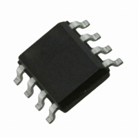
PG-DSO-8
Features
• • • • • • • • • • • • • • • 500V Startup Cell switched off after Start Up Active Burst Mode for lowest Standby Power @ light load controlled by Feedback Signal Fast load jump response in Active Burst Mode 100/67kHz internally fixed switching frequency Auto Restart Mode for Overtemperature Detection Auto Restart Mode for VCC Overvoltage Detection Auto Restart Mode for Overload and Open Loop Auto Restart Mode for VCC Undervoltage Blanking Window for short duration high current User defined Soft Start Minimum of external components required Max Duty Cycle 72% Overall tolerance of Current Limiting < ±5% Internal PWM Leading Edge Blanking Soft switching for low EMI
Description
P-DSO-8-3, -6
The F3 Controller provides Active Burst Mode to reach the lowest Standby Power Requirements 140°C
S1 4.8V
VVCC
t
FB
5.4V
C4
& G5
Auto Restart Mode
C3 Voltage Reference
8.5V
IVCC
7.2mA
Figure 18
t
Auto Restart Mode
1.05mA
VOUT
Max. Ripple < 1%
t
t
The VCC voltage is observed by comparator C1 if 17V is exceeded. The output of C1 is combined with both the output of C11 which checks for SoftS4.8V. Therefore the overvoltage detection is can only active during Soft Start Phase(SoftS 4.8V. This means any small voltage overshoots of VVCC during normal operating cannot trigger the Auto Restart Mode. In order to ensure system reliability and prevent any false activation, a blanking time is implemented before the IC can enter into the Auto Restart Mode. The output of the VCC overvoltage detection is fed into a spike blanking with a time constant of 8.0µs. The other fault detection which can result in the Auto Restart Mode and has this 8.0µs blanking time is the Overtemperature detection. This block checks for a junction temperature of higher than 140°C for malfunction operation.
Figure 17
Signals in Active Burst Mode
Version 1.2
14
02 Sep 2005
�F3 ICE3AS02 / ICE3AS02G / ICE3BS02 / ICE3BS02G
Functional Description
Once the Auto Restart Mode is entered, the internal Voltage Reference is switched off in order to reduce the current consumption of the IC as much as possible. In this mode, the average current consumption is only 300µA as the only working block is the Undervoltage Lockout(UVLO) which controls the Startup Cell by switching on/off at VVCCon/ VVCCoff. As there is no longer a self supply by the auxiliary winding, VCC starts to drop. The UVLO switches on the integrated Startup Cell when VCC falls below 8.5V. It will continue to charge VCC up to 15V whereby it is switched off again and the IC enters into the Start Up Phase. As long as all fault conditions have been removed, the IC will automatically power up as usual with switching cycle at the GATE output after Soft Start duration. Thus the name Auto Restart Mode. Other fault detections which are active in normal operation is the sensing for Overload, Open Loop and VCC undervoltage conditions. In the first 2 cases, FB will rise above 4.8V which will be observed by C4. At this time, S1 is released such that VSoftS can rise from its earlier clamp voltage of 4.4V. If VSoftS exceeds 5.4V which is observed by C3, Auto Restart Mode is entered as both inputs of the gate G5 are high. This charging of the Soft Start capacitor from 4.4V to 5.4V defines a blanking window which prevents the system from entering into Auto Restart Mode un-intentionally during large load jumps. In this event, FB will rise close to 6.5V for a short duration before the loop regulates with FB less than 4.8V. This is the same blanking time window as for the Active Burst Mode and can therefore be adjusted by the external CSoftS. In the case of VCC undervoltage, ie. VCC falls below 8.5V, the IC will be turn off with the Startup Cell charging VCC as described earlier in this section. Once VCC is charged above 15V, the IC will start a new startup cycle. The same procedure applies when the system is under Short Optocoupler fault condition, as it will lead to VCC undervoltage.
Version 1.2
15
02 Sep 2005
�F3 ICE3AS02 / ICE3AS02G / ICE3BS02 / ICE3BS02G
Electrical Characteristics
4
Note:
Electrical Characteristics
All voltages are measured with respect to ground (Pin 8). The voltage levels are valid if other ratings are not violated.
4.1
Note:
Absolute Maximum Ratings
Absolute maximum ratings are defined as ratings, which when being exceeded may lead to destruction of the integrated circuit. For the same reason make sure, that any capacitor that will be connected to pin 7 (VCC) is discharged before assembling the application circuit. Symbol VHV VVCC VFB VSoftS VGate VCS Tj TS PtotDSO8 PtotDIP8 RthJADSO8 RthJADIP8 VESD -0.3 -0.3 -0.3 -0.3 -0.3 -40 -55 Limit Values min. max. 500V 22 6.5 6.5 22 6.5 150 150 0.45 0.90 185 90 3 V V V V V V °C °C W W K/W K/W kV PG-DSO-8, Tamb < 50°C PG-DIP-8, Tamb < 50°C PG-DSO-8 PG-DIP-8 Human body model1) Internally clamped at 11.5V Unit Remarks
Parameter HV Voltage VCC Supply Voltage FB Voltage SoftS Voltage Gate Voltage CS Voltage Junction Temperature Storage Temperature Total Power Dissipation Thermal Resistance Junction-Ambient ESD Capability(incl. HV Pin)
1)
According to EIA/JESD22-A114-B (discharging a 100pF capacitor through a 1.5kΩ series resistor)
4.2
Note:
Operating Range
Within the operating range the IC operates as described in the functional description. Symbol VVCC Limit Values min. max. 21 130 V °C Max value limited due to thermal shut down of controller VVCCoff -25 Unit Remarks
Parameter VCC Supply Voltage
Junction Temperature of Controller TjCon
Datasheet, Version 1.2
16
02 Sep 2005
�F3 ICE3AS02 / ICE3AS02G / ICE3BS02 / ICE3BS02G
Electrical Characteristics 4.3
4.3.1 Note:
Characteristics
Supply Section 1 The electrical characteristics involve the spread of values within the specified supply voltage and junction temperature range TJ from – 25 °C to 130 °C. Typical values represent the median values, which are related to 25°C. If not otherwise stated, a supply voltage of VCC = 15 V is assumed. Symbol min. IVCCstart IVCCcharge1 IVCCcharge2 IStartLeak IVCCsup1 IVCCrestart 0.55 Limit Values typ. 160 1.05 0.88 0.2 5.5 300 max. 220 1.60 20 7.0 µA mA mA µA mA µA IFB = 0 ISofts = 0 VVCC =15V VFB = 3.7V, VSoftS = 4.4V VVCC = 9.5V VFB = 3.7V, VSoftS = 4.4V VVCC =14V VVCC = 0V VVCC =14V VVCC =16V, VHV = 450V Unit Test Condition
Parameter Start Up Current VCC Charge Current Leakage Current of Start Up Cell Supply Current with Inactive Gate Supply Current in Auto Restart Mode with Inactive Gate Supply Current in Active Burst Mode with Inactive Gate VCC Turn-On Threshold VCC Turn-Off Threshold VCC Turn-On/Off Hysteresis
IVCCburst1 IVCCburst2 VVCCon VVCCoff VVCChys
14.2 8.0 -
1.05 0.95 15.0 8.5 6.5
1.25 1.15 15.8 9.0 -
mA mA V V V
4.3.2 Parameter
Supply Section 2 Symbol min. ICE3AS02 ICE3AS02G ICE3BS02 ICE3BS02G IVCCsup2 IVCCsup3 Limit Values typ. 7.0 6.5 max. 8.5 8.0 mA mA VSoftS = 4.4V IFB = 0, CLoad=1nF Unit Test Condition
Supply Current with Active Gate
4.3.3 Parameter
Internal Voltage Reference Symbol min. VREF 6.37 Limit Values typ. 6.50 max. 6.63 V measured at pin FB IFB = 0 Unit Test Condition
Trimmed Reference Voltage
Version 1.2
17
02 Sep 2005
�F3 ICE3AS02 / ICE3AS02G / ICE3BS02 / ICE3BS02G
Electrical Characteristics
4.3.4 Parameter Fixed Oscillator Frequency ICE3AS02 ICE3AS02G ICE3BS02 ICE3BS02G Max. Duty Cycle Min. Duty Cycle PWM-OP Gain Voltage Ramp Max Level VFB Operating Range Min Level VFB Operating Range Max level FB Pull-Up Resistor SoftS Pull-Up Resistor
1)
PWM Section Symbol min. fOSC1 fOSC2 fOSC3 fOSC4 Dmax Dmin AV VMax-Ramp VFBmin VFBmax RFB RSoftS 92 94 61 63 0.67 0 3.5 0.3 16 39 Limit Values typ. 100 100 67 67 0.72 3.7 0.85 0.7 20 50 max. 108 106 73 71 0.77 3.9 4.75 27 62 V V V kΩ kΩ CS=1V, limited by Comparator C41) VFB < 0.3V kHz kHz kHz kHz Tj = 25°C Tj = 25°C Unit Test Condition
The parameter is not subjected to production test - verified by design/characterization Control Unit Symbol min. VSoftSC2 VSoftSclmp VSoftSC3 ISoftSstart VFBC4 VFBC5 VFBC6a 3.85 4.23 5.20 4.62 1.23 3.85 Limit Values typ. 4.00 4.40 5.40 1.3 4.80 1.30 4.00 max. 4.15 4.57 5.60 4.98 1.37 4.15 V V V mA V V V VFB > 5V VFB = 4V VFB > 5V VSoftS = 0V VSoftS > 5.6V VSoftS > 5.6V After Active Burst Mode is entered Unit Test Condition
4.3.5 Parameter
Deactivation Level for SoftS Comparator C7 by C2 Clamped VSoftS Voltage during Normal Operating Mode Activation Limit of Comparator C3 SoftS Startup Current Over Load & Open Loop Detection Limit for Comparator C4 Active Burst Mode Level for Comparator C5 Active Burst Mode Level for Comparator C6a
Datasheet, Version 1.2
18
02 Sep 2005
�F3 ICE3AS02 / ICE3AS02G / ICE3BS02 / ICE3BS02G
Electrical Characteristics
Parameter Active Burst Mode Level for Comparator C6b Overvoltage Detection Limit Thermal Shutdown1) Spike Blanking
1)
Symbol min. VFBC6b VVCCOVP TjSD tSpike 3.25 16.1 130 -
Limit Values typ. 3.40 17.1 140 8.0 max. 3.55 18.1 150 -
Unit V V °C µs
Test Condition After Active Burst Mode is entered VFB > 5V VSoftS < 4.0V
The parameter is not subjected to production test - verified by design/characterization The trend of all the voltage levels in the Control Unit is the same regarding the deviation except VVCCOVP and VVCCPD Current Limiting Symbol min. Vcsth 0.97 Limit Values typ. 1.02 max. 1.07 V dVsense / dt = 0.6V/µs (see Figure 14) Unit Test Condition
Note: 4.3.6
Parameter Peak Current Limitation (incl. Propagation Delay Time of external MOS) Peak Current Limitation during Active Burst Mode Leading Edge Blanking CS Input Bias Current
VCS2 tLEB ICSbias
0.232 -1.0
0.257 220 -0.2
0.282 0
V ns µA VSoftS = 4.4V VCS =0V
Version 1.2
19
02 Sep 2005
�F3 ICE3AS02 / ICE3AS02G / ICE3BS02 / ICE3BS02G
Electrical Characteristics
4.3.7 Parameter GATE Low Voltage Driver Section Symbol min. VGATElow -0.2 GATE High Voltage VGATEhigh GATE Rise Time (incl. Gate Rising Slope) GATE Fall Time GATE Current, Peak, Rising Edge GATE Current, Peak, Falling Edge
1) 2)
Limit Values typ. 0.8 1.6 0.2 11.5 10.5 7.5 150 55 max. 1.2 1.5 2.0 0.7
Unit V V V V V V V V ns ns A A
Test Condition VVCC = 5 V IGate = 5 mA VVCC = 5 V IGate = 20 mA IGate = 0 A IGate = 20 mA IGate = -20 mA VVCC = 20V CL = 4.7nF VVCC = 11V CL = 4.7nF VVCC = VVCCoff + 0.2V CL = 4.7nF VGate = 2V ...9V1) CL = 4.7nF VGate = 9V ...2V1) CL = 4.7nF CL = 4.7nF2) CL = 4.7nF2)
trise tfall IGATE IGATE
-0.5 -
Transient reference value The parameter is not subjected to production test - verified by design/characterization
Version 1.2
20
02 Sep 2005
�F3 ICE3AS02 / ICE3AS02G / ICE3BS02 / ICE3BS02G
Outline Dimension
5
Outline Dimension
PG-DIP-8 (Pb-free Plating Plastic Dual In-Line Outline)
Figure 19
PG-DIP-8 (Pb-free Plating Plastic Dual In-Line Outline)
PG-DSO-8 (Pb-free Plating Plastic Dual Small Outline)
Figure 20
GP-DSO-8 (Pb-free Plating Plastic Dual Small Outline)
Dimensions in mm
Version 1.2
21
02 Sep 2005
�Total Quality Management
Qualität hat für uns eine umfassende Bedeutung. Wir wollen allen Ihren Ansprüchen in der bestmöglichen Weise gerecht werden. Es geht uns also nicht nur um die Produktqualität – unsere Anstrengungen gelten gleichermaßen der Lieferqualität und Logistik, dem Service und Support sowie allen sonstigen Beratungs- und Betreuungsleistungen. Dazu gehört eine bestimmte Geisteshaltung unserer Mitarbeiter. Total Quality im Denken und Handeln gegenüber Kollegen, Lieferanten und Ihnen, unserem Kunden. Unsere Leitlinie ist jede Aufgabe mit „Null Fehlern“ zu lösen – in offener Sichtweise auch über den eigenen Arbeitsplatz hinaus – und uns ständig zu verbessern. Unternehmensweit orientieren wir uns dabei auch an „top“ (Time Optimized Processes), um Ihnen durch größere Schnelligkeit den entscheidenden Wettbewerbsvorsprung zu verschaffen. Geben Sie uns die Chance, hohe Leistung durch umfassende Qualität zu beweisen. Wir werden Sie überzeugen. Quality takes on an allencompassing significance at Semiconductor Group. For us it means living up to each and every one of your demands in the best possible way. So we are not only concerned with product quality. We direct our efforts equally at quality of supply and logistics, service and support, as well as all the other ways in which we advise and attend to you. Part of this is the very special attitude of our staff. Total Quality in thought and deed, towards co-workers, suppliers and you, our customer. Our guideline is “do everything with zero defects”, in an open manner that is demonstrated beyond your immediate workplace, and to constantly improve. Throughout the corporation we also think in terms of Time Optimized Processes (top), greater speed on our part to give you that decisive competitive edge. Give us the chance to prove the best of performance through the best of quality – you will be convinced.
http://www.infineon.com
Published by Infineon Technologies AG
�