IPW60R165CP
CoolMOS® Power Transistor
Features • Lowest figure-of-merit R ONxQg • Ultra low gate charge • Extreme dv/dt rated • High peak current capability • Qualified according to JEDEC1) for target applications • Pb-free lead plating; RoHS compliant
Product Summary V DS @ Tj,max R DS(on),max Q g,typ 650 V
0.165 Ω 39 nC
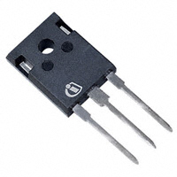
PG-TO247-3
CoolMOS CP is specially designed for: • Hard switching topologies, for Server and Telecom
Type IPW60R165CP
Package PG-TO247-3
Ordering Code SP000095483
Marking 6R165P
Maximum ratings, at T j=25 °C, unless otherwise specified Parameter Continuous drain current Symbol Conditions ID T C=25 °C T C=100 °C Pulsed drain current2) Avalanche energy, single pulse Avalanche energy, repetitive t AR2),3) Avalanche current, repetitive t AR2),3) MOSFET dv /dt ruggedness Gate source voltage I D,pulse E AS E AR I AR dv /dt V GS V DS=0...480 V static AC (f >1 Hz) Power dissipation Operating and storage temperature Mounting torque Rev. 2.2 P tot T j, T stg M3 and M3.5 screws page 1 T C=25 °C T C=25 °C I D=7.9 A, V DD=50 V I D=7.9 A, V DD=50 V Value 21 13 61 522 0.79 7.9 50 ±20 ±30 192 -55 ... 150 60 W °C Ncm 2008-02-18 A V/ns V mJ Unit A
Please note the new package dimensions arccording to PCN 2009-134-A
�IPW60R165CP
Maximum ratings, at T j=25 °C, unless otherwise specified Parameter Continuous diode forward current Diode pulse current 2) Reverse diode d v /dt 4) Symbol Conditions IS I S,pulse dv /dt T C=25 °C Value 12 61 15 V/ns Unit A
Parameter
Symbol Conditions min.
Values typ. max.
Unit
Thermal characteristics Thermal resistance, junction - case Thermal resistance, junction ambient Soldering temperature, wavesoldering only allowed at leads R thJC R thJA leaded 1.6 mm (0.063 in.) from case for 10 s 0.65 62 K/W
T sold
-
-
260
°C
Electrical characteristics, at T j=25 °C, unless otherwise specified Static characteristics Drain-source breakdown voltage Gate threshold voltage V (BR)DSS V GS=0 V, I D=250 µA V GS(th) V DS=V GS, I D=0,79 mA V DS=600 V, V GS=0 V, T j=25 °C V DS=600 V, V GS=0 V, T j=150 °C Gate-source leakage current Drain-source on-state resistance I GSS R DS(on) V GS=20 V, V DS=0 V V GS=10 V, I D=12 A, T j=25 °C V GS=10 V, I D=12 A, T j=150 °C Gate resistance RG f =1 MHz, open drain 600 2.5 3 3.5 V
Zero gate voltage drain current
I DSS
-
-
1
µA
-
10 0.15
100 0.165 nA Ω
-
0.40 1.9
Ω
Rev. 2.2
page 2
2008-02-18
Please note the new package dimensions arccording to PCN 2009-134-A
�IPW60R165CP
Parameter Symbol Conditions min. Dynamic characteristics Input capacitance Output capacitance Effective output capacitance, energy related5) Effective output capacitance, time related6) Turn-on delay time Rise time Turn-off delay time Fall time Gate Charge Characteristics Gate to source charge Gate to drain charge Gate charge total Gate plateau voltage Reverse Diode Diode forward voltage Reverse recovery time Reverse recovery charge Peak reverse recovery current
1)
Values typ. max.
Unit
C iss C oss C o(er)
V GS=0 V, V DS=100 V, f =1 MHz
-
2000 100 83
-
pF
V GS=0 V, V DS=0 V to 480 V C o(tr) t d(on) tr t d(off) tf V DD=400 V, V GS=10V, I D=12 A, R G=3.3 Ω 220 12 5 50 5 ns
Q gs Q gd Qg V plateau V DD=400 V, I D=12 A, V GS=0 to 10 V
-
9 13.0 39 5.0
52 -
nC
V
V SD t rr Q rr I rrm
V GS=0 V, I F=12 A, T j=25 °C
-
0.9 390 7.5 38
1.2 -
V ns µC A
V R=400 V, I F=I S, di F/dt =100 A/µs
-
J-STD20 and JESD22 Pulse width t p limited by T j,max Repetitive avalanche causes additional power losses that can be calculated as P AV=E AR*f. ISD≤ID, di/dt≤200A/µs, VDClink=400V, Vpeak