SPB07N60C3 Cool MOS™ Power Transistor
Feature • New revolutionary high voltage technology • Ultra low gate charge • Periodic avalanche rated • Extreme dv/dt rated • High peak current capability • Improved transconductance
VDS @ Tjmax RDS(on) ID
650 0.6 7.3
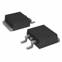
PG-TO263
V Ω A
Type
Package
Ordering Code
Marking 07N60C3
SPB07N60C3
PG-TO263
Q67040-S4394
Maximum Ratings Parameter Symbol Value
Unit
SPB
Continuous drain current
TC = 25 °C TC = 100 °C
ID
A 7.3 4.6
Pulsed drain current, tp limited by Tjmax Avalanche energy, single pulse
ID=5.5A, VDD =50V
ID puls
21.9
A
EAS
230
mJ
Avalanche energy, repetitive tAR limited by Tjmax2)
ID=7.3A, VDD =50V
EAR
0.5
Avalanche current, repetitive tAR limited by Tjmax
Gate source voltage static
IAR
7.3
A
VGS
±20
±30
V
Gate source voltage AC (f >1Hz)
Power dissipation, TC = 25°C
VGS
Ptot
83
W
Operating and storage temperature Reverse diode dv/dt 6)
T j , Tstg dv/dt
-55...+150 15
°C V/ns
Rev. 2.5
Page 1
2005-09-14
�SPB07N60C3
Maximum Ratings Parameter Symbol Value Unit
Drain Source voltage slope
V DS = 480 V, ID = 7.3 A, Tj = 125 °C
dv/dt
50
V/ns
Thermal Characteristics Parameter Symbol min. RthJC RthJC_FP RthJA RthJA_FP RthJA Values typ. max. Unit
Thermal resistance, junction - case Thermal resistance, junction - case, FullPAK Thermal resistance, junction - ambient, leaded Thermal resistance, junction - ambient, FullPAK SMD version, device on PCB: @ min. footprint @ 6 cm 2 cooling area 3)
-
35
1.5 3.9 62 80 62 -
K/W
Soldering temperature, reflow soldering, MSL1 1.6 mm (0.063 in.) from case for 10s
Tsold
-
-
260
°C
Electrical Characteristics, at T j=25°C unless otherwise specified Parameter Symbol Conditions min. Drain-source breakdown voltage V(BR)DSS VGS=0V, ID=0.25mA Drain-Source avalanche V(BR)DS VGS=0V, ID=7.3A breakdown voltage Gate threshold voltage Zero gate voltage drain current VGS(th) I DSS
ID=350µA, VGS=VDS VDS=600V, VGS=0V, Tj=25°C Tj=150°C
Values typ. 700 3 0.5 0.54 1.46 0.8 max. 3.9 600 2.1 -
Unit V
µA 1 100 100 0.6 nA Ω
Gate-source leakage current
I GSS
VGS=30V, VDS=0V VGS=10V, ID=4.6A Tj=25°C Tj=150°C
Drain-source on-state resistance RDS(on)
Gate input resistance
RG
f=1MHz, open drain
Rev. 2.5
Page 2
2005-09-14
�SPB07N60C3
Electrical Characteristics, at Tj = 25 °C, unless otherwise specified Parameter Characteristics
Transconductance Input capacitance Output capacitance Reverse transfer capacitance
Symbol
Conditions min.
Values typ. 6 790 260 16 30 55 6 3.5 60 7 max. 100 15
Unit
g fs Ciss Coss Crss
V DS≥2*I D*RDS(on)max, ID=4.6A V GS=0V, V DS=25V, f=1MHz
-
S pF
Effective output capacitance,4) Co(er) energy related Effective output capacitance,5) Co(tr) time related
Turn-on delay time Rise time Turn-off delay time Fall time
Gate Charge Characteristics Gate to source charge Gate to drain charge Gate charge total Gate plateau voltage Qgs Qgd Qg
V GS=0V, V DS=0V to 480V
td(on) tr td(off) tf
V DD=380V, V GS=0/13V, ID=7.3A, RG=12Ω, Tj=125°C
-
ns
VDD=480V, ID=7.3A
-
3 9.2 21 5.5
27 -
nC
VDD=480V, ID=7.3A, VGS=0 to 10V
V(plateau) VDD=480V, ID=7.3A
V
1Limited only by maximum temperature 2Repetitve avalanche causes additional power losses that can be calculated as PAV=EAR*f. 3Device on 40mm*40mm*1.5mm epoxy PCB FR4 with 6cm² (one layer, 70 µm thick) copper area for drain connection. PCB is vertical without blown air. 4C o(er) is a fixed capacitance that gives the same stored energy as Coss while VDS is rising from 0 to 80% V DSS. 5C o(tr) is a fixed capacitance that gives the same charging time as Coss while V DS is rising from 0 to 80% V DSS.
6I