SPD02N80C3
CoolMOSTM Power Transistor
Features • New revolutionary high voltage technology • Extreme dv/dt rated • High peak current capability • Qualified according to JEDEC1) for target applications • Pb-free lead plating; RoHS compliant • Ultra low gate charge • Ultra low effective capacitances
Product Summary V DS R DS(on)max @ Tj = 25°C Q g,typ 800 2.7 12 V Ω nC
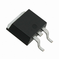
PG-TO252-3
CoolMOSTM 800V designed for: • Industrial application with high DC bulk voltage • Switching Application ( i.e. active clamp forward )
Type SPD02N80C3
Package PG-TO252-3
Marking 02N80C3
Maximum ratings, at T j=25 °C, unless otherwise specified Parameter Continuous drain current Symbol Conditions ID T C=25 °C T C=100 °C Pulsed drain current2) Avalanche energy, single pulse Avalanche energy, repetitive t AR2),3) Avalanche current, repetitive t AR2),3) MOSFET dv /dt ruggedness Gate source voltage I D,pulse E AS E AR I AR dv /dt V GS V DS=0…640 V static AC (f >1 Hz) Power dissipation Operating and storage temperature P tot T j, T stg T C=25 °C T C=25 °C I D=1 A, V DD=50 V I D=2 A, V DD=50 V Value 2 1.2 6 90 0.05 2 50 ±20 ±30 42 -55 ... 150 W °C A V/ns V mJ Unit A
Rev. 2.9
page 1
2008-10-15
�SPD02N80C3
Maximum ratings, at T j=25 °C, unless otherwise specified Parameter Continuous diode forward current Diode pulse current 2) Reverse diode d v /dt 4) Symbol Conditions IS I S,pulse dv /dt T C=25 °C Value 2 6 4 V/ns Unit A
Parameter
Symbol Conditions min.
Values typ. max.
Unit
Thermal characteristics Thermal resistance, junction - case R thJC R thJA Thermal resistance, junction ambient SMD version, device on PCB, minimal footprint SMD version, device on PCB, 6 cm2 cooling area5) T sold reflow MSL1 3 62 K/W
-
35
-
Soldering temperature, reflow soldering
-
-
260
°C
Electrical characteristics, at T j=25 °C, unless otherwise specified Static characteristics Drain-source breakdown voltage Avalanche breakdown voltage Gate threshold voltage Zero gate voltage drain current V (BR)DSS V GS=0 V, I D=250 µA V (BR)DS V GS(th) I DSS V GS=0 V, I D=2 A V DS=V GS, I D=0.12 mA V DS=800 V, V GS=0 V, T j=25 °C V DS=800 V, V GS=0 V, T j=150 °C Gate-source leakage current Drain-source on-state resistance I GSS R DS(on) V GS=20 V, V DS=0 V V GS=10 V, I D=1.2 A, T j=25 °C V GS=10 V, I D=1.2 A, T j=150 °C Gate resistance Rev. 2.9 RG f =1 MHz, open drain page 2 800 2.1 870 3 3.9 5 µA V
-
25 2.4
100 2.7 nA Ω
-
6.5 1.2
Ω 2008-10-15
�SPD02N80C3
Parameter Symbol Conditions min. Dynamic characteristics Input capacitance Output capacitance Effective output capacitance, energy related6) Effective output capacitance, time related7) Turn-on delay time Rise time Turn-off delay time Fall time Gate Charge Characteristics Gate to source charge Gate to drain charge Gate charge total Gate plateau voltage Reverse Diode Diode forward voltage Reverse recovery time Reverse recovery charge Peak reverse recovery current
1) 2)
Values typ. max.
Unit
C iss C oss C o(er)
V GS=0 V, V DS=100 V, f =1 MHz
-
290 13 11
-
pF
V GS=0 V, V DS=0 V to 480 V C o(tr) t d(on) tr t d(off) tf V DD=400 V, V GS=0/10 V, I D=2 A, R G=47 Ω, T j=25 °C 26 25 15 72 18 ns
Q gs Q gd Qg V plateau V DD=640 V, I D=2 A, V GS=0 to 10 V
-
1.5 6 12 5.5
16 -
nC
V
V SD t rr Q rr I rrm
V GS=0 V, I F=I S=2 A, T j=25 °C
-
1 520 2 6
1.2 -
V ns µC A
V R=400 V, I F=I S=2 A, di F/dt =100 A/µs
-
J-STD20 and JESD22 Pulse width t p limited by T j,max Repetitive avalanche causes additional power losses that can be calculated as P AV=E AR*f. ISD≤ID, di/dt≤400A/µs, VDClink = 400V, Vpeak