SPW11N60S5 Cool MOS™ Power Transistor
Feature • New revolutionary high voltage technology • Ultra low gate charge • Periodic avalanche rated • Extreme dv/dt rated • Ultra low effective capacitances • Improved transconductance
VDS RDS(on) ID
600 0.38 11
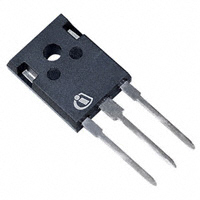
PG-TO247
V Ω A
Type SPW11N60S5
Package PG-TO247
Ordering Code Q67040-S4239
Marking 11N60S5
Maximum Ratings Parameter Symbol ID Value Unit
Continuous drain current
TC = 25 °C TC = 100 °C
A 11 7
Pulsed drain current, tp limited by Tjmax Avalanche energy, single pulse
I D = 5.5 A, VDD = 50 V
I D puls EAS
22 340 0.6 11 ±20
±30
mJ
Avalanche energy, repetitive tAR limited by Tjmax1) EAR
I D = 11 A, VDD = 50 V
Avalanche current, repetitive tAR limited by Tjmax I AR Gate source voltage VGS Gate source voltage AC (f >1Hz)
Power dissipation, T C = 25°C
A V W °C
VGS Ptot T j , T stg
125 -55... +150
Operating and storage temperature
Rev. 2.4
Page 1
2008-02-11
Please note the new package dimensions arccording to PCN 2009-134-A
�SPW11N60S5
Maximum Ratings Parameter Drain Source voltage slope
V DS = 480 V, ID = 11 A, Tj = 125 °C
Symbol dv/dt
Value 20
Unit V/ns
Thermal Characteristics Parameter Thermal resistance, junction - case Thermal resistance, junction - ambient, leaded Symbol min. RthJC RthJA Values typ. max. 1 62 K/W Unit
Soldering temperature, wavesoldering 1.6 mm (0.063 in.) from case for 10s
Tsold
-
-
260
°C
Electrical Characteristics, at Tj=25°C unless otherwise specified Parameter Symbol Conditions min. Drain-source breakdown voltage V(BR)DSS VGS=0V, ID=0.25mA Drain-Source avalanche breakdown voltage Gate threshold voltage Zero gate voltage drain current VGS(th) IDSS
ID=500µΑ, VGS=V DS VDS=600V, VGS=0V, Tj=25°C, Tj=150°C
Values typ. 700 4.5 0.34 0.92 29 max. 5.5 600 3.5 -
Unit V
V(BR)DS VGS=0V, ID=11A
µA 25 250 100 0.38 nA Ω
Gate-source leakage current
IGSS
VGS=20V, VDS=0V VGS=10V, ID=7A, Tj=25°C Tj=150°C
Drain-source on-state resistance RDS(on)
Gate input resistance
RG
f=1MHz, open Drain
Rev. 2.4
Page 2
2008-02-11
Please note the new package dimensions arccording to PCN 2009-134-A
�SPW11N60S5
Electrical Characteristics , at Tj = 25 °C, unless otherwise specified Parameter Characteristics
Transconductance Input capacitance Output capacitance Reverse transfer capacitance
Symbol
Conditions min.
Values typ. 6 1460 610 21 45 85 130 35 150 20 max. 225 30
Unit
g fs Ciss Coss Crss
V DS≥2*I D*RDS(on)max,
ID=7A
-
S pF
V GS=0V, V DS=25V, f=1MHz
Effective output capacitance, 2) Co(er) energy related Effective output capacitance, 3) Co(tr) time related
Turn-on delay time Rise time Turn-off delay time Fall time
V GS=0V, V DS=0V to 480V
pF
t d(on) tr t d(off) tf
V DD=350V, V GS=0/10V,
ID=11A, R G=6.8Ω
-
ns
Gate Charge Characteristics Gate to source charge Qgs Gate to drain charge Gate charge total Gate plateau voltage Qgd Qg
VDD=350V, ID=11A
-
10.5 24 41.5 8
54 -
nC
VDD=350V, ID=11A, VGS=0 to 10V
V(plateau) VDD=350V, ID=11A
V
1Repetitve avalanche causes additional power losses that can be calculated as P =EAR*f. AV 2C o(er) is a fixed capacitance that gives the same stored energy as Coss while VDS is rising from 0 to 80% V DSS. 3C o(tr) is a fixed capacitance that gives the same charging time as Coss while V DS is rising from 0 to 80% V DSS.
Rev. 2.4
Page 3
2008-02-11
Please note the new package dimensions arccording to PCN 2009-134-A
�SPW11N60S5
Electrical Characteristics , at Tj = 25 °C, unless otherwise specified Parameter Inverse diode continuous forward current Inverse diode direct current, pulsed Inverse diode forward voltage Reverse recovery time Reverse recovery charge VSD trr Qrr
VGS=0V, IF=IS VR=350V, IF =IS , di F/dt=100A/µs
Symbol IS ISM
Conditions min.
TC=25°C
Values typ. 1 650 7.9 max. 11 22 1.2 1105 -
Unit A
V ns µC
Typical Transient Thermal Characteristics Symbol
Thermal resistance R th1 R th2 R th3 R th4 R th5 R th6 0.015 0.03 0.056 0.197 0.216 0.083 K/W
Value typ.
Unit
Symbol
Value typ.
Unit
Thermal capacitance Cth1 Cth2 Cth3 Cth4 Cth5 Cth6 0.0001878 0.0007106 0.000988 0.002791 0.007285 0.063 Ws/K
Tj
R th1
R th,n
T case
E xternal H eatsink
P tot (t) C th1 C th2 C th,n
T am b
Rev. 2.4
Page 4
2008-02-11
Please note the new package dimensions arccording to PCN 2009-134-A
�SPW11N60S5
1 Power dissipation
Ptot = f (TC)
140
SPW11N60S5
2 Safe operating area
ID = f ( V DS ) parameter : D = 0 , T C=25°C
10 2
W
A
120 110 100 10 1
Ptot
80 70 60 50 40 30 20 10 0 0 20 40 60 80 100 120 10 -1 10 0
ID
90
tp = 0.001 ms tp = 0.01 ms tp = 0.1 ms tp = 1 ms DC
°C
160
10 -2 0 10
10
1
10
2
TC
10 V VDS
3
3 Transient thermal impedance
ZthJC = f (t p) parameter: D = tp/T
10
1
4 Typ. output characteristic
ID = f (VDS); Tj=25°C parameter: tp = 10 µs, VGS
35
K/W A
10 0 25 10 -1
20V 12V 10V
ZthJC
ID
20
9V
10 -2
10 -3
D = 0.5 D = 0.2 D = 0.1 D = 0.05 D = 0.02 D = 0.01 single pulse
15
8V
10
7V
5
6V
10 -4 -7 10
10
-6
10
-5
10
-4
10
-3
s tp
10
-1
0 0
5
10
15
VDS
25
V
Rev. 2.4
Page 5
2008-02-11
Please note the new package dimensions arccording to PCN 2009-134-A
�SPW11N60S5
5 Typ. output characteristic
ID = f (VDS); Tj=150°C parameter: tp = 10 µs, VGS
18
6 Typ. drain-source on resistance
RDS(on)=f(ID) parameter: Tj=150°C, V GS
2
A
20V 12V 10V
9V 8V
14 12 10
mΩ RDS(on)
ID
1 8
7V
6 4
6V
0.5
20V 12V 10V 9V 8V 7V 6V
2 0 0 0 0
5
10
15
V VDS
25
2
4
6
8
10
12
14
A ID
18
7 Drain-source on-state resistance
RDS(on) = f (Tj) parameter : ID = 7 A, VGS = 10 V
Ω
2.1
SPW11N60S5
8 Typ. transfer characteristics
ID= f ( VGS ); V DS≥ 2 x ID x RDS(on)max parameter: tp = 10 µs
32
A
1.8 1.6 1.4 1.2 1 0.8 0.6 98% 0.4 0.2 0 -60 -20 20 60 100
°C
RDS(on)
24
ID
20
25 °C 150 °C
16
12
8 typ 4
180
0 0
4
8
12
V
20
Tj
VGS
Rev. 2.4
Page 6
2008-02-11
Please note the new package dimensions arccording to PCN 2009-134-A
�SPW11N60S5
9 Typ. gate charge
VGS = f (QGate) parameter: ID = 11 A pulsed
16
V 0.2 VDS max
SPW11N60S5
10 Forward characteristics of body diode
IF = f (VSD) parameter: Tj , tp = 10 µs
10 2
SPW11N60S5
A
12 0.8 VDS max
VGS
10 1
8
6
IF
10 0 Tj = 25 °C typ Tj = 150 °C typ Tj = 25 °C (98%) Tj = 150 °C (98%) 10 20 30 40 50
nC
10
4
2 10 -1 0
0 0
65
0.4
0.8
1.2
1.6
2
2.4 V
3
QGate
VSD
11 Avalanche SOA
IAR = f (tAR) par.: Tj ≤ 150 °C
11
12 Avalanche energy
EAS = f (Tj) par.: ID = 5.5 A, V DD = 50 V
350
A
mJ
9 8 7 6 5 4 3 2 1 0 -3 10 10
-2
Tj (START) =125°C Tj (START) =25°C
250
EAS
200 150 100 50
-1 0 1 2 4 µs 10 tAR
IAR
10
10
10
10
0 20
40
60
80
100
120
°C
160
Tj
Rev. 2.4
Page 7
2008-02-11
Please note the new package dimensions arccording to PCN 2009-134-A
�SPW11N60S5
13 Drain-source breakdown voltage
V(BR)DSS = f (Tj)
720
SPW11N60S5
14 Avalanche power losses
PAR = f (f ) parameter: E AR=0.6mJ
300
V
W
V(BR)DSS
680
PAR
660 640
200
150 620 600 580 50 560 540 -60 04 10
5 6
100
-20
20
60
100
°C
180
10
Hz f
10
Tj
15 Typ. capacitances
C = f (VDS) parameter: V GS=0V, f=1 MHz
10 4
16 Typ. Coss stored energy
Eoss=f(VDS)
7.5
pF
Ciss
10 3
µJ
6 5.5
Eoss
10 2
5 4.5 4
C
Coss
3.5 3 2.5
10
1
Crss
2 1.5 1 0.5
10 0 0
100
200
300
400
V
600
0 0
100
200
300
400
V
600
VDS
VDS
Rev. 2.4
Page 8
2008-02-11
Please note the new package dimensions arccording to PCN 2009-134-A
�SPW11N60S5
Definition of diodes switching characteristics
Rev. 2.4
Page 9
2008-02-11
Please note the new package dimensions arccording to PCN 2009-134-A
�1 6 S5
G
Rev. 2.4
P
8 2 11
Please note the new package dimensions arccording to PCN 2009-134-A
�1 6 S5
Rev. 2.4
Page 11
2008-02-11
Please note the new package dimensions arccording to PCN 2009-134-A
�Data sheet erratum PCN 2009-134-A
New package outlines TO-247
1
New package outlines TO-247
Assembly capacity extension for CoolMOSTM technology products assembled in lead-free package PG-TO247-3 at subcontractor ASE (Weihai) Inc., China (Changes are marked in blue.)
Figure 1
Outlines TO-247, dimensions in mm/inches Rev. 2.0, 2010-02-01
Final Data Sheet Erratum
�


 工商网监
湘ICP备2023018690号
工商网监
湘ICP备2023018690号
