Infineon® Power LED Driver TLD5095EL
DC/DC Boost, Buck-Boost, SEPIC controller
Datasheet
Rev. 1.1, 2009-12-16
Automotive Power
�TLD5095EL
Table of Contents
Table of Contents
1 2 3 3.1 3.2 4 4.1 4.2 4.3 5 5.1 5.2 6 6.1 6.2 7 7.1 7.2 8 8.1 8.2 9 9.1 9.2 10 10.1 11 12 Overview . . . . . . . . . . . . . . . . . . . . . . . . . . . . . . . . . . . . . . . . . . . . . . . . . . . . . . . . . . . . . . . . . . . . . . . 3 Block Diagram . . . . . . . . . . . . . . . . . . . . . . . . . . . . . . . . . . . . . . . . . . . . . . . . . . . . . . . . . . . . . . . . . . . 4 Pin Configuration . . . . . . . . . . . . . . . . . . . . . . . . . . . . . . . . . . . . . . . . . . . . . . . . . . . . . . . . . . . . . . . . 5 Pin Assignment . . . . . . . . . . . . . . . . . . . . . . . . . . . . . . . . . . . . . . . . . . . . . . . . . . . . . . . . . . . . . . . . . . . 5 Pin Definitions and Functions . . . . . . . . . . . . . . . . . . . . . . . . . . . . . . . . . . . . . . . . . . . . . . . . . . . . . . . . 5 General Product Characteristics . . . . . . . . . . . . . . . . . . . . . . . . . . . . . . . . . . . . . . . . . . . . . . . . . . . . Absolute Maximum Ratings . . . . . . . . . . . . . . . . . . . . . . . . . . . . . . . . . . . . . . . . . . . . . . . . . . . . . . . . . Functional Range . . . . . . . . . . . . . . . . . . . . . . . . . . . . . . . . . . . . . . . . . . . . . . . . . . . . . . . . . . . . . . . . . Thermal Resistance . . . . . . . . . . . . . . . . . . . . . . . . . . . . . . . . . . . . . . . . . . . . . . . . . . . . . . . . . . . . . . . 7 7 8 8
Boost Regulator . . . . . . . . . . . . . . . . . . . . . . . . . . . . . . . . . . . . . . . . . . . . . . . . . . . . . . . . . . . . . . . . . 9 Description . . . . . . . . . . . . . . . . . . . . . . . . . . . . . . . . . . . . . . . . . . . . . . . . . . . . . . . . . . . . . . . . . . . . . . 9 Electrical Characteristics . . . . . . . . . . . . . . . . . . . . . . . . . . . . . . . . . . . . . . . . . . . . . . . . . . . . . . . . . . 10 Oscillator and Synchronization . . . . . . . . . . . . . . . . . . . . . . . . . . . . . . . . . . . . . . . . . . . . . . . . . . . . 11 Description . . . . . . . . . . . . . . . . . . . . . . . . . . . . . . . . . . . . . . . . . . . . . . . . . . . . . . . . . . . . . . . . . . . . . 11 Electrical Characteristics . . . . . . . . . . . . . . . . . . . . . . . . . . . . . . . . . . . . . . . . . . . . . . . . . . . . . . . . . . 12 Enable and Dimming Function . . . . . . . . . . . . . . . . . . . . . . . . . . . . . . . . . . . . . . . . . . . . . . . . . . . . 14 Description . . . . . . . . . . . . . . . . . . . . . . . . . . . . . . . . . . . . . . . . . . . . . . . . . . . . . . . . . . . . . . . . . . . . . 14 Electrical Characteristics . . . . . . . . . . . . . . . . . . . . . . . . . . . . . . . . . . . . . . . . . . . . . . . . . . . . . . . . . . 15 Linear Regulator . . . . . . . . . . . . . . . . . . . . . . . . . . . . . . . . . . . . . . . . . . . . . . . . . . . . . . . . . . . . . . . . 17 Description . . . . . . . . . . . . . . . . . . . . . . . . . . . . . . . . . . . . . . . . . . . . . . . . . . . . . . . . . . . . . . . . . . . . . 17 Electrical Characteristics . . . . . . . . . . . . . . . . . . . . . . . . . . . . . . . . . . . . . . . . . . . . . . . . . . . . . . . . . . 18 Protection and Diagnostic Functions . . . . . . . . . . . . . . . . . . . . . . . . . . . . . . . . . . . . . . . . . . . . . . . 19 Description . . . . . . . . . . . . . . . . . . . . . . . . . . . . . . . . . . . . . . . . . . . . . . . . . . . . . . . . . . . . . . . . . . . . . 19 Electrical Characteristics . . . . . . . . . . . . . . . . . . . . . . . . . . . . . . . . . . . . . . . . . . . . . . . . . . . . . . . . . . 23 Application Information . . . . . . . . . . . . . . . . . . . . . . . . . . . . . . . . . . . . . . . . . . . . . . . . . . . . . . . . . . 24 Further Application Information . . . . . . . . . . . . . . . . . . . . . . . . . . . . . . . . . . . . . . . . . . . . . . . . . . . . . . 28 Revision History . . . . . . . . . . . . . . . . . . . . . . . . . . . . . . . . . . . . . . . . . . . . . . . . . . . . . . . . . . . . . . . . 29 Package Outlines . . . . . . . . . . . . . . . . . . . . . . . . . . . . . . . . . . . . . . . . . . . . . . . . . . . . . . . . . . . . . . . 30
Datasheet
2
Rev. 1.1, 2009-12-16
�DC/DC Boost, Buck-Boost, SEPIC controller TLD5095EL
TLD5095EL
1
Features • • • • • • • • • • • • • • • • •
Overview
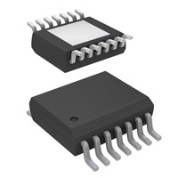
Wide Input Voltage Range from 4.75 V to 45 V Constant Current or Constant Voltage Regulation Drives LEDs in Boost (B2G), Buck-Boost (B2B) and SEPIC Topology Very Low Shutdown Current: IQ< 10 µA Flexible Switching Frequency Range, 100 kHz to 500 kHz Synchronization with external clock source Output Open Circuit Diagnostic Output PWM Dimming PG-SSOP-14 (e-Pad) Internal Soft Start 300mV High Side Current Sense to ensure highest flexibility and LED current accuracy Internal 5 V Low Drop Out Voltage Regulator Wide LED current range via simple adaptation of external components Available in a small thermally enhanced PG-SSOP-14 (e-Pad) package Output Overvoltage Protection Over Temperature Shutdown Automotive AEC Qualified Green Product (RoHS) Compliant
Description The TLD5095EL is a smart LED boost controller with built in protection and diagnostic features. The main function of this device is to regulate a constant LED current. The constant current regulation is especially beneficial for LED color accuracy and longer lifetime. The controller concept of the TLD5095EL allows a multi-purpose usage such as Boost, Buck-Boost and SEPIC configuration with various load current levels by simply adjusting the external components. The TLD5095EL has a PWM output for dimming a LED load. The diagnostics are communicated on a status output (pin ST) to indicate a fault condition such as an LED open circuit. The switching frequency is adjustable in the range of 100 kHz to 500 kHz and can be synchronized to an external clock source. The TLD5095EL features an enable function reducing the shut-down current consumption to VIVCC,RTH,d
– –
Note: Within the functional range the IC operates as described in the circuit description. The electrical characteristics are specified within the conditions given in the related electrical characteristics table.
4.3
Thermal Resistance
Note: This thermal data was generated in accordance with JEDEC JESD51 standards. For more information, go to www.jedec.org. Pos. 4.3.1 4.3.2 4.3.3 4.3.4 Parameter Junction to Case
1) 2) 1) 3)
Symbol Min.
Limit Values Typ. – 47 54 64 Max. 10 – – – – – – –
Unit K/W K/W K/W K/W
Conditions
Junction to Ambient
RthJC RthJA RthJA RthJA
2s2p 1s0p + 600 mm2 1s0p + 300 mm2
1) Not subject to production test, specified by design. 2) Specified RthJC value is simulated at natural convection on a cold plate setup (all pins and exposed pad are fixed to ambient temperature). Ta=25°C, IC is dissipating 1W. 3) Specified RthJA value is according to JEDEC 2s2p (JESD 51-7) + (JESD 51-5) and JEDEC 1s0p (JESD 51-3) + heatsink area at natural convection on FR4 board; The device was simulated on a 76.2 x 114.3 x 1.5mm board. The 2s2p board has 2 outer copper layers (2 x 70µm Cu) and 2 inner copper layers (2 x 35µm Cu), A thermal via (diameter = 0.3mm and 25µm plating) array was applied under the exposed pad and connected the first outer layer (top) to the first inner layer and second outer layer (bottom) of the JEDEC PCB. Ta=25°C, IC is dissipating 1W.
Datasheet
8
Rev. 1.1, 2009-12-16
�TLD5095EL
Boost Regulator
5
5.1
Boost Regulator
Description
The TLD5095 regulator is suitable for boost, buck-boost and SEPIC configurations. The constant output current is especially useful for light emitting diode (LED) applications. The boost regulator function is implemented by a pulse width modulated (PWM) current mode controller. The PWM current mode controller uses the peak current through the external power switch and error in the output current to determine the appropriate pulse width duty cycle (on time) for constant output current. The current mode controller it provides a PWM signal to an internal gate driver which then outputs the same PWM signal to external n-channel enhancement mode metal oxide field effect transistor (MOSFET) power switch. The current mode controller also has built-in slope compensation to prevent sub-harmonic oscillations which is a characteristic of current mode controllers operating at high duty cycles (>50% duty). An additional built-in feature is an integrated soft start that limits the current through the inductor and external power switch during initialization. The soft start function gradually increases the inductor and switch current over 1 ms (typical) to minimize potential overvoltage at the output.
OV FB OVFB
H when OVFB >1.25V
TLD5095
High when IVCC < 4.0V UV IVCC
VRef =
1.25V
COMP = VRef 4.0V Output Stage OFF when Low
FBH
x1
EA
gmEA
IEA
Current Comp
NOR High when lEA - ISLOPE - I CS > 0 OFF when H Low when Tj > 175 °C R
FBL
> 1
Gate Driver Supply
IVCC
R
& &
Q
INV 1 Gate Driver
SWO
VRef
0.3V
=
Soft start
& &
Q S Q
I SLOPE
Oscillator FREQ/ SYNC
I
Slope Comp
PWM-FF Q NAND 2
Current Sense
ICS
t
Clock
S
SWCS
Error -FF
&
SGND
Figure 3
Boost Regulator Block Diagram
Datasheet
9
Rev. 1.1, 2009-12-16
�TLD5095EL
Boost Regulator
5.2
1)
Electrical Characteristics
VIN = 6V to 40V; 4.5V ≤ VFBH ≤ 40V, 4.5V ≤ VFBL ≤ 40V, Tj = -40 °C to +150 °C, all voltages with respect to ground,
positive current flowing into pin; (unless otherwise specified) Pos. Parameter Symbol Min. Boost Regulator: 5.2.1 5.2.2 Feedback Reference Voltage Voltage Line Regulation Limit Values Typ. Max. Unit Conditions
VREF
∆VREF /∆VIN
0.28 –
0.30 –
0.32 0.15
V %/V
VIN = 19 V; VREF= VFBH -VFBL VIN = 6 to 19 V; VBO= 30 V; IBO = 500 mA
Figure 21
5.2.3
Voltage Load Regulation
∆VREF /∆IBO
–
–
5
%/A
VIN = 6 V; VBO = 30V; IBO = 100 to 500 mA
Figure 21
5.2.4
Switch Peak Over Current Threshold Maximum Duty Cycle Maximum Duty Cycle Soft Start Ramp Feedback Input Current Switch Current Sense Input Current Input Undervoltage Shutdown Input Voltage Startup
VSWCS
130
150
170
mV
VIN = 6 V VFBH = VFBL = 5 V VCOMP = 3.5V
Fixed frequency mode Synchronization mode
5.2.5 5.2.6 5.2.7 5.2.8 5.2.9 5.2.10 5.2.11
DMAX,fixed 90 DMAX,sync 88 tSS 350 IFBx ISWCS VIN,off VIN,on
-10 10 3.75 –
93 – 1000 -50 50 – –
95 – 1500 -100 100 – 4.75
% % µs µA µA V V
VFB rising from 5% to 95% of VFB, typ. VFBH - VFBL = 0.3 V VSWCS = 150 mV VIN decreasing VIN increasing
Gate Driver for Boost Switch 5.2.12 5.2.13 5.2.14 5.2.15 5.2.16 Gate Driver Peak Sourcing Current1) Gate Driver Peak Sinking Current1) Gate Driver Output Rise Time Gate Driver Output Fall Time Gate Driver Output Voltage1)
ISWO,SRC ISWO,SNK tR,SWO tF,SWO VSWO
– – – – 4.5
380 550 30 20 –
– – 60 40 5.5
mA mA ns ns V
VSWO = 3.5V VSWO = 1.5V CL,SWO = 3.3nF; VSWO = 1V to 4V CL,SWO = 3.3nF; VSWO = 1V to 4V CL,SWO = 3.3nF;
1) Not subject to production test, specified by design
Datasheet
10
Rev. 1.1, 2009-12-16
�TLD5095EL
Oscillator and Synchronization
6
6.1
Oscillator and Synchronization
Description
R_OSC vs. switching frequency The internal oscillator is used to determine the switching frequency of the boost regulator. The switching frequency can be selected from 100 kHz to 500 kHz with an external resistor to GND. To set the switching frequency with an external resistor the following formula can be applied.
R FREQ =
(141 × 10 [ ])× ( f
− 12 s Ω
1
FREQ
[1s ])
− 3 . 5 × 10 3 [Ω ]
(
) [Ω ]
In addition, the oscillator is capable of changing from the frequency set by the external resistor to a synchronized frequency from an external clock source. If an external clock source is provided on the pin FREQ/SYNC, then the internal oscillator synchronizes to this external clock frequency and the boost regulator switches at the synchronized frequency. The synchronization frequency capture range is 250 kHz to 500 kHz.
T LD5095
FREQ / SYNC
Oscillator Clock Frequency Detector
Multiplexer
PWM Logic
Gate Driver
SW O
VCLK
R FREQ
Oscillator_BlkDiag_SyncFixedMode .vsd
Figure 4
Oscillator and Synchronization Block Diagram and Simplified Application Circuit
Figure 5
Synchronization Timing Diagram
Datasheet
11
Rev. 1.1, 2009-12-16
�TLD5095EL
Oscillator and Synchronization
6.2
Electrical Characteristics
VIN = 6V to 40V; 4.5V ≤ VFBH ≤ 40V, 4.5V ≤ VFBL ≤ 40V, Tj = -40 °C to +150 °C, all voltages with respect to ground,
positive current flowing into pin; (unless otherwise specified) Pos. Parameter Symbol Min. Oscillator: 6.2.1 6.2.2 Oscillator Frequency Oscillator Frequency Adjustment Range FREQ / SYNC Supply Current Frequency Voltage Limit Values Typ. Max. Unit Conditions
fFREQ fFREQ
250 100
300 –
350 500
kHz kHz
RFREQ = 20kΩ
17% internal tolerance + external resistor tolerance
6.2.3 6.2.4
IFREQ VFREQ
– 1.16
– 1.24
-700 1.32
µA V
VFREQ = 0 V fFREQ = 100 kHz
Synchronization 6.2.5 6.2.6 6.2.7 6.2.8 Synchronization Frequency Capture Range Synchronization Signal High Logic Level Valid Synchronization Signal Low Logic Level Valid Synchronization Signal Logic High Pulse Width
fSYNC VSYNC,H VSYNC,L
250 3.0 –
– – – –
500 – 0.8 –
kHz V V ns
–
1)
1)
tSYNC,PWH 200
1)
1) Synchronization of external PWM ON signal to falling edge
Datasheet
12
Rev. 1.1, 2009-12-16
�TLD5095EL
Oscillator and Synchronization Typical Performance Characteristics of Oscillator Switching Frequency fSW versus Frequency Select Resistor to GND RFREQ/SYNC
600
500
400 fFREQ [kHz]
T j = 25 °C
300
200
100
0 0 10 20 30 40 50 60 70 80 RFREQ/SYNC [kohm]
Datasheet
13
Rev. 1.1, 2009-12-16
�TLD5095EL
Enable and Dimming Function
7
7.1
Enable and Dimming Function
Description
The enable function powers on or off the device. A valid logic low signal on enable pin EN/PWMI powers off the device and current consumption is less than 10 µA. A valid logic high enable signal on enable pin EN/PWMI powers on the device. The enable function features an integrated pull down resistor which ensures that the IC is shut down and the power switch is off in case the enable pin EN is left open. In addition to the enable function described above, the EN/PWMI pin detects a pulse width modulated (PWM) input signal that is fed through to an internal gate driver. The internal gate driver outputs the same PWM signal on the PWMO pin to an external n-channel enhancement mode MOSFET for PWM dimming an LED load. PWM dimming an LED is a commonly practiced dimming method to prevent color shift in an LED light source. Moreover the PWM output function may also be used for to drive other types of loads besides LED. The enable and PWM input function share the same pin. Therefore a valid logic low signal at the EN/PWMI pin needs to differentiate between an enable power off signal or an PWM low signal. The device differentiates between an enable off command and PWM dimming signal by requiring the signal at the EN/PWMI pin to stay low for a minimum of 8 ms.
Figure 6
Block Diagram and Simplified Application Circuit Enable and LED Dimming
Datasheet
14
Rev. 1.1, 2009-12-16
�TLD5095EL
Enable and Dimming Function
Figure 7
Timing Diagram Enable and LED Dimming
7.2
Electrical Characteristics
VIN = 6V to 40V; 4.5V ≤ VFBH ≤ 40V, 4.5V ≤ VFBL ≤ 40V, Tj = -40 °C to +150 °C, all voltages with respect to ground,
positive current flowing into pin; (unless otherwise specified) Pos. Parameter Symbol Limit Values Min. Enable/PWM Input: 7.2.1 7.2.2 7.2.3 Enable/PWMI Turn On Threshold Enable/PWMI Turn Off Threshold Enable/PWMI Hysteresis Typ. – – 200 0.8 400 Max. V V mV – – – Unit Conditions
VEN/PWMI,ON
3.0
VEN/PWMI,OFF – VEN/PWMI,HYS 50
Datasheet
15
Rev. 1.1, 2009-12-16
�TLD5095EL
Enable and Dimming Function
VIN = 6V to 40V; 4.5V ≤ VFBH ≤ 40V, 4.5V ≤ VFBL ≤ 40V, Tj = -40 °C to +150 °C, all voltages with respect to ground,
positive current flowing into pin; (unless otherwise specified) Pos. 7.2.4 7.2.5 7.2.6 7.2.7 7.2.8 Parameter Enable/PWMI High Input Current Enable/PWMI Low Input Current Enable Turn Off Delay Time PWMI Min Duty Time Enable Startup Time Symbol Limit Values Min. Typ. – 0.1 10 – – Max. 30 1 12 – – µA µA ms µs µs – – 8 4 100 Unit Conditions
IEN/PWMI,H IEN/PWMI,L tEN,OFF,DEL tPWMI,H tEN,START
VEN/PWMI = 16.0 V VEN/PWMI = 0.5 V
–
Gate Driver for Dimming Switch: 7.2.9 7.2.10 7.2.11 7.2.12 7.2.13 PWMO Gate Driver Peak Sourcing Current1) PWMO Gate Driver Peak Sinking Current1) PWMO Gate Driver Output Rise Time PWMO Gate Driver Output Fall Time PWMO Gate Driver Output Voltage
IPWMO,SRC IPWMO,SNK tR,PWMO tF,PWMO VPWMO
– – – – 4.5
230 370 50 30 –
– – 100 60 5.5
mA mA ns ns V
VPWMO = 3.5V VPWMO = 1.5V CL,PWMO = 3.3nF; VPWMO = 1V to 4V CL,PWMO = 3.3nF; VPWMO = 1V to 4V CL,PWMO = 3.3nF;
Current Consumption 7.2.14 7.2.15 Current Consumption, Shutdown Mode Current Consumption, Active Mode2)
Iq_off Iq_on
– –
– –
10 7
µA mA
VEN/PWMI = 0.8 V; Tj ≤ 105C; VIN = 16V VEN/PWMI ≥ 4.75 V; IBO = 0 mA; VIN = 16V VSWO = 0% Duty
1) Not subject to production test, specified by design 2) Dependency on switching frequency and gate charge of boost and dimming switch.
Datasheet
16
Rev. 1.1, 2009-12-16
�TLD5095EL
Linear Regulator
8
8.1
Linear Regulator
Description
The internal linear voltage regulator supplies the internal gate drivers with a typical voltage of 5 V and current up to 50 mA. An external output capacitor with low ESR is required on pin IVCC for stability and buffering transient load currents. During normal operation the external boost and dimming MOSFET switches will draw transient currents from the linear regulator and its output capacitor. Proper sizing of the output capacitor must be considered to supply sufficient peak current to the gate of the external MOSFET switches. Integrated undervoltage protection for the external switching MOSFET: An integrated undervoltage reset threshold circuit monitors the linear regulator output voltage (VIVCC) and resets the device in case the output voltage falls below the IVCC undervoltage reset switch OFF threshold (VIVCC,RTH,d). The undervoltage reset threshold for the IVCC pin helps to protect the external switches from excessive power dissipation by ensuring the gate drive voltage is sufficient to enhance the gate of an external logic level n-channel MOSFET.
IN
14
1
IVCC
Linear Regulator
EN / PWMI
13
Gate Drivers
LinReg_BlckDiag.vsd
Figure 8
Voltage Regulator Block Diagram and Simplified Application Circuit
Datasheet
17
Rev. 1.1, 2009-12-16
�TLD5095EL
Linear Regulator
8.2
Electrical Characteristics
VIN = 6V to 40V; 4.5V ≤ VFBH ≤ 40V, 4.5V ≤ VFBL ≤ 40V, Tj = -40 °C to +150 °C, all voltages with respect to ground,
positive current flowing into pin; (unless otherwise specified) Pos. 8.2.1 8.2.2 8.2.3 8.2.4 8.2.5 8.2.6 8.2.7 8.2.8 Parameter Output Voltage Output Current Limitation Drop out Voltage Symbol Min. Limit Values Typ. 5 Max. 5.4 90 1.4 – 0.5 – – – – – 4.5 V mA V µF Ω mV V V 6 V ≤ VIN ≤ 45 V 0.1 mA ≤ IIVCC ≤ 50 mA 4.6 51 Unit Conditions
VIVCC ILIM
VDR Output Capacitor CIVCC 0.47 Output Capacitor ESR RIVCC,ESR Undervoltage Reset Headroom VIVCC,HDRM 100
Undervoltage Reset Threshold VIVCC,RTH,d Undervoltage Reset Threshold VIVCC,RTH,i 4.0 –
VIN = 13.5 V VIVCC = 4.5V IIVCC = 50mA 1)
2)
f = 10kHz VIVCC decreasing VIVCC - VIVCC,RTH,d VIVCC decreasing VIVCC increasing
1) Measured when the output voltage VCC has dropped 100 mV from its nominal value. 2) Minimum value given is needed for regulator stability; application might need higher capacitance than the minimum.
Datasheet
18
Rev. 1.1, 2009-12-16
�TLD5095EL
Protection and Diagnostic Functions
9
9.1
Protection and Diagnostic Functions
Description
The TLD5095EL has integrated circuits to diagnose and protect against output overvoltage, open load, open feedback and overtemperature faults. In case any of the four fault conditions occur the Status output ST will output an active logic low signal to communicate that a fault has occurred. During an overvoltage or open load condition the gate driver outputs SWO and PWMO will turn off. Figure 11 illustrates the various open load and open feedback conditions. In the event of an overtemperature condition (Figure 14) the integrated thermal shutdown function turns off the gate drivers and internal linear voltage regulator. The typical junction shutdown temperature is 175°C. After cooling down the IC will automatically restart operation. Thermal shutdown is an integrated protection function designed to prevent immediate IC destruction and is not intended for continuous use in normal operation.
Input
Output Overvoltage Open Load
Protection and Diagnostic Circuit
Output
OR
Open Feedback
SWO and PWMO Gate Driver Off
Overtemperature
OR
Input Undervoltage
Linear Regualtor Off
Pro_Diag_BlckDiag.vsd
Figure 9
Protection and Diagnostic Function Block Diagram
Input Condition Overvoltage Open Load Open Feedback Overtemperature
Level* False True False True False True False True
ST H L H L H L H L
Output SWO PWMO IVCC Sw* H or Sw * Active L L Active Sw* H or Sw * Active L L Active Sw* H or Sw * Active L L Active Sw* H or Sw * Active L L Shutdown
Pro_Diag_TT.vsd
*Note: Sw = Switching False = Condition does not exist True = Condition does exist
Figure 10 Datasheet
Status Output Truth Table 19 Rev. 1.1, 2009-12-16
�TLD5095EL
Protection and Diagnostic Functions
VBO Open Circuit 3
Output Open Circuit Conditions Open Circuit Condition 1 2 3 4 Fault Condition Open FBH Open FBL Open VBO Open PWMO Fault Threshold Voltage VREF -20 to -100 mV 0.5 to 1.0 V VFBx < VFBx,min = 4.5V Detected by overvoltage
TLD5095
ROVH Overvoltage Compartor OVFB RFB 9 ROVL
Open Circuit 1
Open Circuit 2 D1 D2 D3
VOVFB,TH
VREF
Feedback Voltage Error Amplifier
FBH
D4 6 + VREF D5 D6 D7 D8 D9 D10 Open Circuit 4 TDIM Open FBL Open FBH Open VBO
FBL
7
Max Threshold = 1.0 V
Min Threshold = 0.5 V Typical V REF = 0.3 V Max Threshold = -20 mV Min Threshold = -100 mV
PWMO
5
Figure 11
Open Load and Open Feedback Conditions
example: VOUT,max=40V
1.25mA
VOVFB
VOVP,max
TLD5095
OVFB
9
ROVH
40V ≅ 33.2kΩ 1.25mA
Overvoltage Protection ACTIVE
VOVFB,TH 1.25V
ROVL
GND
12
1kΩ 1.25V
Overvoltage Protection is disabled t
Figure 12
Overvoltage Protection description
Datasheet
20
Rev. 1.1, 2009-12-16
�TLD5095EL
Protection and Diagnostic Functions
Status Output Timing Diagram
Startup Normal Thermal Shutdown 1 Overvoltage 2 Open Load / Feedback 3 Shutdown
VIVCC
VIVCC,RTH,i VIVCC,RTH ,d
TJ
TJ,SD
T J,SD,HYST
t
1
VOVFB ≥ VOVFB,TH VOVFB < V OVFB,T L
VBO
2
t
VFBH -VFBL
VREF,2 0.3 V Typ VREF,1 tSS tSS
3
t
t
tSD tSD tSD
VST
t
Figure 13
Status Output Timing Diagram
Datasheet
21
Rev. 1.1, 2009-12-16
�TLD5095EL
Protection and Diagnostic Functions
VEN/PWMI
H L t
Tj
TjSD TjSO
∆Τ
Ta
t
VSWO
t
ILED
Ipeak t
VPWMO
t
VST and VIVCC
5V t
Device OFF Normal Operation Overtemp Fault
ON
Overtemp Fault
ON
Overtemp ON Fault
Overtemp Fault
Figure 14 Datasheet
Device overtemperature protection behavior 22 Rev. 1.1, 2009-12-16
�TLD5095EL
Protection and Diagnostic Functions
9.2
Electrical Characteristics
VIN = 6V to 40V; 4.5V ≤ VFBH ≤ 40V, 4.5V ≤ VFBL ≤ 40V, Tj = -40 °C to +150 °C, all voltages with respect to ground,
positive current flowing into pin; (unless otherwise specified) Pos. Parameter Symbol Min. Status Output: 9.2.1 9.2.2 9.2.3 9.2.4 Status Output Voltage Low Status Sink Current Limit Status Output Current Status Delay Time Limit Values Typ. Max. Unit Conditions
VST,LOW IST,MAX IST,HIGH tSD
– 2 – 8
– – – 10
0.4 – 1 12
V mA µA ms
IST = 1mA VST = 1V VST = 5V
–
Temperature Protection: 9.2.5 9.2.6 Over Temperature Shutdown Over Temperature Shutdown Hystereses
Tj,SD 160 Tj,SD,HYST –
175 15
190 –
°C °C
– –
Overvoltage Protection: 9.2.7 9.2.8 9.2.9 9.2.10 Output Over Voltage Feedback Threshold Increasing Output Over Voltage Feedback Hysteresis Over Voltage Reaction Time Over Voltage Feedback Input Current
VOVFB,TH
1.21
1.25 – – 0.1
1.29 150 10 1
V mV µs µA
– Output Voltage decreasing Output Voltage decreasing
VOVFB,HYS 50 tOVPRR IOVFB
2 -1
VOVFB = 1.25 V
Open Load and Open Feedback Diagnostics 9.2.11 9.2.12 Open Load/Feedback Threshold Open Feedback Threshold
VREF,1,3 VREF,2
-100 0.5
– –
-20 1
mV V
VREF = VFBH - VFBL
Open Circuit 1 or 3
VREF = VFBH - VFBL
Open Circuit 2
Note: Integrated protection functions are designed to prevent IC destruction under fault conditions described in the data sheet. Fault conditions are considered as “outside” normal operating range. Protection functions are not designed for continuous repetitive operation.
Datasheet
23
Rev. 1.1, 2009-12-16
�TLD5095EL
Application Information
10
Application Information
Note: The following information is given as a hint for the implementation of the device only and shall not be regarded as a description or warranty of a certain functionality, condition or quality of the device.
IBO DR V VBATT C1 C2 TSW
2
L1 CIN
VIN
LBO
DBO ISW
VBO CBO
RFB
IN SWO SWCS
VREF
D1 D2 D3
14
3
RC S VCC SGND IVC C / VC C OVFB RST
4
ROVH
D4 D5
IC2 Microcontroller (e.g. XC866)
Input Output Output
9
10 13 11 8
ST
IC 1 TLD5095
FBH FBL
6 7
ROVL
D6 D7 D8 D9 D10
EN / PWMI FREQ / SYNC COMP IVCC PWMO
5
CC OM P
ILED
TD IM
1
RFR EQ
RC OM P
CIVC C
GND
12
Provisional Parts
Figure 15
LED Low Side Return Application Circuit (Boost to GND, B2G)
Part Number LW W5SM SS3H10 EEEFK 1H101GP X7R
MLC C CC N PZC105 KBW X7 R
Reference Designator D 1 - 10 D BO CIN , C BO CCOMP C IVCC IC 1 IC 2 LBO RCOMP R FB R FREQ, R ST ROVH ROVL R CS TDIM ,TSW
Value White Schottky , 3 A, 100 V R 100 uF, 50V 10 nF 1uF , 6.3V --100 uH 10 kΩ, 1% 820 mΩ , 1% 20 kΩ, 1% 33.2 k Ω, 1% 1 k Ω, 1% 50 mΩ, 1% Dual N -ch enh .
alternativ: 100V N-ch, 35A
Manufacturer Osram Vishay Panasonic EPCOS EPCOS Infineon Infineon Coilcraft Panasonic Panasonic Panasonic Panasonic Panasonic Panasonic Infineon Infineon Infineon
Type LED Diode Capacitor Capacitor Capacitor IC IC Inductor Resistor Resistor Resistor Resistor Resistor Resistor Transistor Transistor Transistor
Quantity 10 1 2 1 1 1 1 1 1 1 2 1 1 1 1 2 2
TLD 5095 XC866 MSS1278T-104ML_ ERJ3EKF 1002V ERJ14BQFR82U ERJ3EKF 2002V ERJ3EKF 3322V ERJ3EKF 1001V ERJB 1CFR 05U IPG15N06S3L-45 IPD35N10S3L-26 BSP 318S
alternativ : 60V N-ch, 2.6A
Figure 16 Datasheet
Bill of Materials for LED Low Side Return Application Circuit 24 Rev. 1.1, 2009-12-16
�TLD5095EL
Application Information
L filter DR V VBATT C1 C2 CIN VIN
L1
CSEPIC
DBO
ISW L2 SWO SWCS TSW
2
RFB
CBO
VREF
14
IN
Provisional Parts
3
ILED
RC S
VCC SGND IVC C / VC C OVFB RST
4
R OVH
D1 D2
IC2 Microcontroller (e.g. XC866)
Input Output Output
9
10 13 11 8
ST
IC 1 TLD5095
FBH FBL
6 7
R OVL
D3 D4 D5 D6 D7 D8
EN / PWMI FREQ / SYNC COMP
CC OM P IVCC RFR EQ RC OM P PWMO GND
12 5 1
DPOL C IVC C
RPOL
D9 D 10
T D IM
Figure 17
SEPIC Application Circuit
Part Number LW W5SM SS3H10 X7R, Low ESR EEEFK1H101GP X7R
MLCC CCNPZC105KBW X7R
Reference Designator D1 - 10 DBO CSEPIC CIN , CBO CCOMP CIVCC IC1 IC2 L1 , L2
Value White Schottky, 3 A, 100 VR 3.3 uF, 20V 100 uF, 50V 10 nF 1uF , 6.3V --22 uH
alternativ: coupled inductor
Manufacturer Osram Vishay EPCOS Panasonic EPCOS EPCOS Infineon Infineon Coilcraft Coilcraft Panasonic Infineon Panasonic Panasonic Panasonic Panasonic Panasonic Infineon Infineon Infineon
Type LED Diode Capacitor Capacitor Capacitor Capacitor IC IC Inductor Inductor Resistor Diode Resistor Resistor Resistor Resistor Resistor Transistor Transistor Transistor
Quantity 10 1 1 2 1 1 1 1 2 1 2 1 1 2 1 1 1 1 2 2
TLD5095 XC866 MSS1278T-223ML MSD1278-223MLD ERJ3EKF1002V BAS1603W ERJ14BQFR82U ERJ3EKF2002V ERJ3EKF3322V ERJ3EKF1001V ERJB1CFR05U IPG15N06S3L-45 IPD35N10S3L-26 BSP318S
RCOMP, RPOL DPOL RFB RFREQ, RST ROVH ROVL RCS TDIM,TSW
10 kΩ, 1% 80V Diode 820 mΩ, 1% 20 kΩ, 1% 33.2 kΩ, 1% 1 kΩ, 1% 50 mΩ, 1% Dual N-ch enh.
alternativ: 100V N-ch, 35A
alternativ : 60V N-ch, 2.6A
Figure 18 Datasheet
Bill of Materials for SEPIC Application Circuit 25 Rev. 1.1, 2009-12-16
�TLD5095EL
Application Information
CBO
VIN DR V VBATT C1 C2 L1 CIN
D 10 R FB
D9
D8
D7
D6
D5
D4
D3
D2
D1
TD IM2
DZ
RD IM2
R D IM1
Provisional Parts
LBO TD IM1
5
DBO ISW
ILED
VOU T PWMO SWO SWCS
6 2 3
TSW
FBH FBL IN SGND OVFB
4
RC S ROVH
VCC
7 14
IC2 Microcontroller (e.g. XC866)
Input Output Output
IVCC/VCC RST
10 13 11 8
9
ST
IC 1 TLD5095
ROVL
EN / PWMI FREQ / SYNC COMP IVCC
CC OM P CIVC C RFR EQ RC OM P
1
GND
12
Figure 19
LED High Side Return Application Circuit (Boost to Vbatt, B2B)
Reference Designator D1 - 10 DBO DZ CBO CIN CCOMP CIVCC IC1 IC2 LBO RCOMP, RDIM1, RDIM2 RFB RFREQ, RST ROVH ROVL RCS TDIM1,TDIM2 Value White Schottky, 3 A, 100 VR 5V Zener Diode 100 uF, 80V 100 uF, 50V 10 nF 1 uF, 6.3V --100 uH 10 kΩ, 1% 820 mΩ, 1% 20 kΩ, 1% 33.2 kΩ, 1% 1 kΩ, 1% 50 mΩ, 1% 60V Dual N-ch (3.1A) and P-ch. enh. (2A)
alternativ: 100V N-ch (0.37A), alternativ: 60V P-ch (1.9A)
Manufacturer Osram Vishay -Panasonic Panasonic EPCOS EPCOS Infineon Infineon Coilcraft Panasonic Panasonic Panasonic Panasonic Panasonic Panasonic Infineon Infineon Infineon Infineon Infineon Infineon
Part Number LW W5AP SS3H10 -EEVFK1K101Q EEEFK1H101GP X7R
MLCC CCNPZC105KBW X7R
Type Diode Diode Diode Capacitor Capacitor Capacitor Capacitor IC IC Inductor Resistor Resistor Resistor Resistor Resistor Resistor Transistor Transistor Transistor Transistor Transistor Transistor
Quantity 10 1 1 1 1 1 1 1 1 1 3 1 2 1 1 1 1 1 1
AppDiagLED _HSR_HSSBOM .vsd
TLD5095 XC866 MSS1278T-104ML_ ERJ3EKF1002V ERJ14BQFR82U ERJ3EKF2002V ERJP06F5102V ERJ3EKF1001V ERJB1CFR05U BSO615CG BSP123 BSP171P IPD35N10S3L-26 IPD30N06S4L-23 BSP318S
TSW
N-ch, OptiMOS-T2 100V, 35A alternativ: 60V N-ch, 30A
1 1 1
alternativ : 60V N-ch, 2.6A
Figure 20 Datasheet
Bill of Materials for LED High Side Return Application Circuit 26 Rev. 1.1, 2009-12-16
�TLD5095EL
Application Information
IBO DRV VBATT C1 C2 SWO
14 2
L1 CIN
VIN
LBO ISW
DBO
VBO CBO
ILoad constant VOUT
RL TSW
IN IVCC SWCS
3
Provisional Parts
1
VCC or V IVCC
RCS
4
CIVCC
SGND
ROVH
IC2 Microcontroller (e.g. XC866)
Input Output Output
OVFB RST
9
10
ST
IC1 TLD5095
FBH
6
ROVL
RFB1
13 11 8
EN / PWMI FREQ / SYNC COMP FBL PWMO
7
RFB2
VREF
CCOMP
RFREQ
RCOMP
GND
12
5
RFB3
Figure 21
Boost Voltage Application Circuit
Reference Designator D1 - 10 DBO CBO CIN CCOMP CIVCC IC1 IC2 LBO RCOMP RFB1,RFB3 RFB2 RFREQ, RST ROVH ROVL RCS TSW Value White Schottky, 3 A, 100 VR 100 uF, 80V 100 uF, 50V 10 nF 1 uF, 6.3V --100 uH 10 kΩ, 1% 51 kΩ, 1% 1 kΩ, 1% 20 kΩ, 1% 33.2 kΩ, 1% 1 kΩ, 1% 50 mΩ, 1% N-ch, OptiMOS-T2 100V Manufacturer Osram Vishay Panasonic Panasonic EPCOS EPCOS Infineon Infineon Coilcraft Panasonic Panasonic Panasonic Panasonic Panasonic Panasonic Panasonic Infineon Part Number LW W5AP SS3H10 EEVFK1K101Q EEEFK1H101GP X7R
MLCC CCNPZC105KBW X7R
Type Diode Diode Capacitor Capacitor Capacitor Capacitor IC IC Inductor Resistor Resistor Resistor Resistor Resistor Resistor Resistor Transistor
Quantity 10 1 1 1 1 1 1 1 1 1 1 1 2 1 1 1 1
TLD5095 XC866 MSS1278T-104ML_ ERJ3EKF1002V ERJ3EKF5102V ERJ3EKF1001V ERJ3EKF2002V ERJ3EKF3322V ERJ3EKF1001V ERJB1CFR05U IPD35N10S3L-26
Figure 22
Bill of Materials for Boost Voltage Application Circuit
Note: The application drawings and corresponding bill of materials are simplified examples. Optimization of the external components must be done accordingly to specific application requirements.
Datasheet
27
Rev. 1.1, 2009-12-16
�TLD5095EL
Application Information
10.1
Further Application Information
In fixed frequency mode where an external resistor configures the switching frequency the minimum boost inductor is given by the formula in Figure 23. • • • • LMIN = Minimum Inductance Required During Fixed Frequency Operation VBO = Boost Output Voltage RCS = Current Sense Resistor fFREQ = Switching Frequency
V BO [ V ] × R CS [ Ω ] L MIN ≥ ----------------------------------------------------------------–3 106 ×10 [ V ] × f FREQ [ Hz ]
Figure 23
Minimum Inductance Required During Fixed Frequency Operation (B2G configuration)
In synchronization mode where an external clock source configures the switching frequency the minimum boost inductor is given by the formula in Figure 24. • • • LSYNC = Minimum Inductance Required During Synchronization Operation VBO = Boost Output Voltage RCS = Current Sense Resistor
V BO [ V ] × R CS [ Ω ] L SYNC ≥ ---------------------------------------------------------–3 106 ×10 [ V ] × 250kHz
Figure 24 •
Minimum Inductance Required During Synchronization Operation (B2G configuration)
For further information you may contact http://www.infineon.com/
Datasheet
28
Rev. 1.1, 2009-12-16
�TLD5095EL
Revision History
11
Revision 1.1
Revision History
Date 2009-12-16 Changes • • • • Cover sheet updated Package naming updated Figure 2 updated Exposed Pad pin description updated
1.0
2009-11-30
Initial Datasheet
Datasheet
29
Rev. 1.1, 2009-12-16
�TLD5095EL
Package Outlines
12
Package Outlines
0.35 x 45˚
Stand Off (1.45)
1.7 MAX.
3.9 ±0.11)
0.1 C D
0 ... 0.1
0.19 +0.06
0.08 C 6 ±0.2
0.65 0.25 ±0.05 2)
C
0.64 ±0.25
D 0.2
8˚ MAX.
M
0.15 M C A-B D 14x
D 8x
A
14 8
Bottom View 3 ±0.2
1 7
1
7
B 0.1 C A-B 2x
Exposed Diepad
14
8
4.9 ±0.11)
Index Marking
1) Does not include plastic or metal protrusion of 0.15 max. per side 2) Does not include dambar protrusion
PG-SSOP-14-1,-2,-3-PO V02
2.65 ±0.2
PG-SSOP-14
Figure 25
PG-SSOP-14
Green Product (RoHS compliant) To meet the world-wide customer requirements for environmentally friendly products and to be compliant with government regulations the device is available as a green product. Green products are RoHS-Compliant (i.e Pb-free finish on leads and suitable for Pb-free soldering according to IPC/JEDEC J-STD-020).
For further package information, please visit our website: http://www.infineon.com/packages. Datasheet 30
Dimensions in mm Rev. 1.1, 2009-12-16
�Edition 2009-12-16 Published by Infineon Technologies AG 81726 Munich, Germany © 2009 Infineon Technologies AG All Rights Reserved. Legal Disclaimer The information given in this document shall in no event be regarded as a guarantee of conditions or characteristics. With respect to any examples or hints given herein, any typical values stated herein and/or any information regarding the application of the device, Infineon Technologies hereby disclaims any and all warranties and liabilities of any kind, including without limitation, warranties of non-infringement of intellectual property rights of any third party. Information For further information on technology, delivery terms and conditions and prices, please contact the nearest Infineon Technologies Office (www.infineon.com). Warnings Due to technical requirements, components may contain dangerous substances. For information on the types in question, please contact the nearest Infineon Technologies Office. Infineon Technologies components may be used in life-support devices or systems only with the express written approval of Infineon Technologies, if a failure of such components can reasonably be expected to cause the failure of that life-support device or system or to affect the safety or effectiveness of that device or system. Life support devices or systems are intended to be implanted in the human body or to support and/or maintain and sustain and/or protect human life. If they fail, it is reasonable to assume that the health of the user or other persons may be endangered.
�