Low Dropout Linear LED Driver
TLE 4240-2/3 M
Features • • • • • • • • • • • Typ. 58 mA constant output current Low dropout voltage Tiny SMD package PG-SCT595-5 Open load detection (Version TLE 4240-3 M only) 45 V input voltage operation range Safe operation area monitoring Output protected against short circuit to GND and supply Reverse polarity protection Wide temperature range: -40 °C ≤ Tj ≤ 150 °C Overtemperature shutdown Suitable for use in automotive electronics
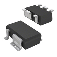
PG-SCT-595
Functional Description The TLE 4240-2/3 M is a monolithic integrated low dropout linear constant current source. It is designed to supply white or color LEDs in order to achive constant brightness and extended LED lifetime independent from supply voltage or LED forward voltage class. Protection circuits prevent from damage to the device in case of overload, short circuit, reverse polarity and overheat. The LEDs connected are protected against reverse polarity transients as well as against voltages up to 45 V. The Safe Operation Area (SOA) monitoring function limits the output current in case of a very high drop voltage across the regulator. For details see graph “Output Current versus Drop Voltage”. Version TLE 4240-3 M is equipped with a status output indicating an open load failure condition. The TLE 4240-2/3 M is supplied in a space-saving PG-SCT595-5 package offering minimal thermal resistance.
Type TLE 4240-2 M TLE 4240-3 M
Datasheet
Package PG-SCT595-5 PG-SCT595-5
1
Remark – Open load detection
Marking 42 43
Rev. 1.1, 2006-12-07
�TLE 4240-2/3 M
n.c. GND I
1 5 2 3 4
Pinout.vsd
ST GND GND Q I
1 5 2 3 4
P inout.vsd
GND
Q
TLE 4240-2 M
TLE 4240-3 M
Figure 1 Table 1 1 1 n.c. ST
Pin Configuration (top view) Pin Definitions and Functions Version TLE 4240-2 M only: Internally not connected. Version TLE 4240-3 M only: Status output; open collector output. Low level indicates open load. Connect to a positive voltage rail with an external pull-up resistor. Leave open, if not needed. Ground; connect to heatsink area. Interconnect with pin 5. Input; IC supply Output; Ground; connect to heatsink area. Interconnect with pin 2.
Pin No. Symbol Function
2 3 4 5
GND I Q GND
Datasheet
2
Rev. 1.1, 2006-12-07
�TLE 4240-2/3 M
TLE 4240-2 M Figure 2 Block Diagram
TLE 4240-3 M
VBAT
TLE 4264 Voltage Regulator
5V µC 4k7 I/O
Open Load
ST I
Open Load Status Output at Version TLE 4240-3 only Q
TLE 4240-2 TLE 4240-3
GND
TLE4240-2_A pplication.vsd
Figure 3
Datasheet
Typical Application Circuit
3 Rev. 1.1, 2006-12-07
�TLE 4240-2/3 M
Table 2 Parameter Input I Voltage Current Output Q Voltage Current
Absolute Maximum Ratings Symbol Limit Values Min. Max. 45 – 40 – 12 – – – – – 150 150 V mA V mA V mA kV kV kV kV °C °C – internally limited – internally limited – internally limited TLE 4240-2 M; HBM 1) TLE 4240-2 M; CDM 2) TLE 4240-3 M; HBM 1) TLE 4240-3 M; CDM 2) – – Unit Remarks
-40 °C ≤ Tj ≤ 150 °C
VI II VQ IQ VST IST VESD,HBM VESD,CDM VESD,HBM VESD,CDM Tj Tstg
-16 – -1 – -0.3 – 4 2 2 2 -40 -50
Status ST (TLE 4240-3 M) Voltage Current ESD Susceptibility ESD Resistivity ESD Resistivity Temperatures Junction temperature Storage temperature
1) ESD susceptibility “human body model (HBM)” according to JESD22-A114. 2) ESD susceptibility “charged device model (CDM)” according to JESD22-C101
Note: Stresses above the ones listed here may cause permanent damage to the device. Exposure to absolute maximum rating conditions for extended periods may affect device reliability. Integrated protection functions are designed to prevent IC destruction under fault conditions described in the data sheet. Fault conditions are considered as “outside” normal operating range. Protection functions are not designed for continuous repetitive operation.
Datasheet
4
Rev. 1.1, 2006-12-07
�TLE 4240-2/3 M
Table 3 Parameter Input voltage
Functional Range Symbol Limit Values Min. Max. 45 15 150 V V °C – – – 3 – -40 Unit Remarks
Status output voltage (Version TLE 4240-3 M only) Junction temperature
VI VST Tj
Table 4 Parameter
Thermal Resistance Symbol Typ. Limit Unit Values Remarks A: footprint only1) A = 300 mm 1) A = 600 mm 1) measured to pin 5
Junction ambient
Rth,j-a
179 99 87
K/W K/W K/W K/W
Junction pin 5
Rth,j-pin5
26
1) Mounted an a PCB 80 × 80 × 1.5 mm3, horizontal position, zero airflow.
Table 5 Parameter
Electrical Characteristics Symbol Limit Values Min. Typ. Max. Unit Test Condition
VI = 13.5 V; VQ = 6 V; -40 °C ≤ Tj ≤ 150 °C; unless otherwise specified
Regulator: Output current
IQ
51 46
57 58 0.5
63 70 0.7
mA mA V
Dropout voltage Vdr = VI - VQ
Vdr
–
Tj = 100 °C 9 V ≤ VI ≤ 16 V Tj ≤ 125 °C IQ = 40 mA
Datasheet
5
Rev. 1.1, 2006-12-07
�TLE 4240-2/3 M
Table 5 Parameter
Electrical Characteristics (cont’d) Symbol Limit Values Min. Typ. – – 7 30 Max. – – 10 40 mA mA mA mA -5 -5 Unit Test Condition
VI = 13.5 V; VQ = 6 V; -40 °C ≤ Tj ≤ 150 °C; unless otherwise specified
Reverse output current
IQ
Current consumption Iq = II - IQ Current consumption open load Version TLE 4240-3 M
Iq Iq
– –
VI = -16 V VQ = 0 V VI = 0 V VQ = 16 V Vdr = 1 V IQ = 0 mA
Open Load Detection (Version TLE 4240-3 M only): Lower status switching threshold VIQ,L = VI - VQ
VIQ,L
–
–
0.8
V
Ramping down (VI - VQ)
Status Output ST (Version TLE 4240-3 M only): Status low voltage Status sink current limitation Status leakage current
VST,low IST,MAX IST,high
– 1.5 –
– – –
0.4 – 2
V mA µA
IST = 1 mA IQ = 5 mA VST = 1 V VST = 5 V (VI - VQ) > 1 V
Datasheet
6
Rev. 1.1, 2006-12-07
�TLE 4240-2/3 M
Typical Performance Characteristics Current Consumption Iq vs. Drop Voltage Vdr = (VI - VQ)
Iq-V dr.vsd
Current Consumption Iq vs. Output Current IQ
Iq-IQ.vsd
I q [ mA]
T j = 25 °C
I q [ mA]
8
VQ = 4.5 V VQ = 7 V
16
Tj = -40 °C
12
6
T j = 25 °C
4
8
2
VQ = 11 V VQ = 22 V
0 1 2 3 4
4
T j = 150 °C
0 20 40 60
V dr [V]
IQ [mA]
Output Current IQ vs. Input Voltage VI ;VQ = 6 V
IQ-VI.vsd
Dropout Voltage Vdr vs. Junction Temperature Tj
0.7
VDR,MIN-TJ.VSD
I Q [ mA]
60
Tj = 25 °C
VQ = 6 V
V dr,min
[V]
50
0.5
T j = 125 °C
40 0.4
I Q = 50 mA
30
0.3
20
0.2
IQ = 40 mA
0
10
20
30
40
0.1 -40 -20
0
20
40
60 80 100 120 140
VI [V]
T j [°C]
Datasheet
7
Rev. 1.1, 2006-12-07
�TLE 4240-2/3 M
Typical Performance Characteristics Output Current IQ vs. Junction Temperature Tj
IQ-Tj.vsd
Output Current IQ vs. Drop Voltage Vdr (SOA)
SOA .vsd
70
IQ VI = 13.5 V VQ = 7 V
[mA]
IQ
[mA]
VQ = 7 V T j = 25 °C
60 60 50 55 40 50 30 45 -40 -20 0 20 40 60 80 100 120 140 0 8 16 24 32
T j [°C]
Vdr [V]
Reverse Current IQ versus Reverse Input Voltage VI
IQrev-V I.vsd
Reverse Current II versus Reverse Input Voltage VI
IIrev-V I.vsd
IQ
[mA]
VQ = 0 V
II
[mA]
VQ = 0 V
-0.5
-10
-1
Tj = -40 °C T j = 25 °C Tj = 150 °C
-20
-1.5
-30
-2
-40
-32
-24
-16
-8
0
-32
-24
-16
-8
0
VI [V]
VI [V]
Datasheet
8
Rev. 1.1, 2006-12-07
�TLE 4240-2/3 M
Typical Performance Characteristics Reverse Output Current IQ versus Output Voltage VQ
IQrev-VQ.vsd
Current Consumption Iq in open load condition vs. Tj
Iq,NL-Tj.vsd
IQ
[mA]
VI = 0 V
Iq
[mA]
VI = 13.5 V Q : open
-1
32
TLE 4240-3 (w/ status output ST)
-2
24
T j = -40 °C
-3 16
-4
T j = 150 °C
8 TLE 4240-2 (no status output)
0
8
16
24
32
-40 -20
0
20
40
60
80 100 120 140
VQ [V]
T j [°C]
Datasheet
9
Rev. 1.1, 2006-12-07
�TLE 4240-2/3 M
Package Outline
Footprint Reflow Soldering
Footprint Wave Soldering
Figure 4
PG-SCT595-5
Find all packages, sorts of packing and others at Infineon Internet Page “Packages”: http://www.infineon.com/packages. SMD = Surface Mounted Device Datasheet 10 Dimensions in mm Rev. 1.1, 2006-12-07
�Edition 2006-12-07 Published by Infineon Technologies AG, 81726 München, Germany © Infineon Technologies AG 2006. All Rights Reserved. Attention please! The information given in this data sheet shall in no event be regarded as a guarantee of conditions or characteristics (“Beschaffenheitsgarantie”). With respect to any examples or hints given herein, any typical values stated herein and/or any information regarding the application of the device, Infineon Technologies hereby disclaims any and all warranties and liabilities of any kind, including without limitation warranties of non-infringement of intellectual property rights of any third party. Information For further information on technology, delivery terms and conditions and prices please contact your nearest Infineon Technologies Office (www.infineon.com). Warnings Due to technical requirements components may contain dangerous substances. For information on the types in question please contact your nearest Infineon Technologies Office. Infineon Technologies Components may only be used in life-support devices or systems with the express written approval of Infineon Technologies, if a failure of such components can reasonably be expected to cause the failure of that life-support device or system, or to affect the safety or effectiveness of that device or system. Life support devices or systems are intended to be implanted in the human body, or to support and/or maintain and sustain and/or protect human life. If they fail, it is reasonable to assume that the health of the user or other persons may be endangered.
�
很抱歉,暂时无法提供与“TLE4240-2M”相匹配的价格&库存,您可以联系我们找货
免费人工找货