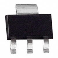
0
登录后你可以
  • 下载海量资料
  • 学习在线课程
  • 观看技术视频
  • 写文章/发帖/加入社区
会员中心
创作中心
发布
  • 发文章

  • 发资料

  • 发帖

  • 提问

  • 发视频

创作活动
TLE42664G

TLE42664G

  • 厂商:

    INFINEON

  • 封装:

  • 描述:

    TLE42664G - Low Dropout Fixed Voltage Regulator - Infineon Technologies AG

  • 详情介绍
  • 数据手册
  • 价格&库存
TLE42664G 数据手册
Data Sheet, Rev. 1.01, September 2009 TLE42664 Low Dropout Fixed Voltage Regulator Automotive Power Low Dropout Fixed Voltage Regulator TLE42664G 1 Features • • • • • • • • • • • • Overview Output Voltage 5 V ±2 % up to Output Currents of 50 mA Output Voltage 5 V ±3 % up to Output Currents 100 mA Very Low Dropout Voltage Very Low Current Consumption: typ. 40 µA Enable Input Output Current Limitation Reverse Polarity Protection Overtemperature Shutdown Wide Temperature Range From -40 °C up to 150 °C Suitable for Use in Automotive Electronics Green Product (RoHS compliant) AEC Qualified PG-SOT223-4 Description The TLE42664 is a monolithic integrated low dropout fixed voltage regulator for load currents up to 100 mA. It is the 1-to-1 replacement product for the TLE4266-2. It is functional compatible to the TLE4266, but has a reduced quiescent current of typ. 40µA. The TLE42664 is especially designed for applications requiring very low standby currents, e.g. with a permanent connection to the car’s battery. It can be disabled/enabled by the integrated EN pin. The device is available in the small surface mounted PG-SOT223-4 package and is pin compatible to the TLE4266-2 and the TLE4266. The device is designed for the harsh environment of automotive applications. Therefore it is protected against overload, short circuit and overtemperature conditions by the implemented output current limitation and the overtemperature shutdown circuit. The TLE42664 can be also used in all other applications requiring a stabilized 5 V voltage. An input voltage up to 45 V is regulated to VQ,nom = 5 V with a precision of ±3 %. An accuracy of ±2 % is kept for load currents up to 50 mA. A logical “HIGH” at the ENABLE pin enables the device. Type TLE42664G Data Sheet Package PG-SOT223-4 2 Marking 42664 Rev. 1.01, 2009-09-30 TLE42664 Block Diagram 2 Block Diagram Temperature Sensor Ι Saturation Control and Protection Circuit Q Control Amplifier Adjustment Bandgap Reference Buffer EN GND GND AEB02874-2 Figure 1 Block Diagram Data Sheet 3 Rev. 1.01, 2009-09-30 TLE42664 Pin Configuration 3 3.1 Pin Configuration Pin Assignment PG-SOT223-4 GND 4 1 2 3 Ι EN Q AEP02872-2 Figure 2 Pin Configuration (top view) 3.2 Pin No. 1 2 Pin Definitions and Functions PG-SOT223-4 Symbol Function I EN Input block to ground directly at the IC with a ceramic capacitor Enable Input high level enables the device; low level disables the device; integrated pull-down resistor Output block to ground with a capacitor close to the IC terminals, respecting the values given for its capacitance and ESR in “Functional Range” on Page 5 Ground / Heat Slug internally connected to leadframe and GND; connect to GND and heatsink area 3 Q 4 / Heat Slug GND Data Sheet 4 Rev. 1.01, 2009-09-30 TLE42664 General Product Characteristics 4 4.1 General Product Characteristics Absolute Maximum Ratings Absolute Maximum Ratings1) Tj = -40 °C to 150 °C; all voltages with respect to ground, (unless otherwise specified) Pos. Parameter Symbol Min. Input I, Enable EN 4.1.1 Output Q 4.1.2 4.1.3 4.1.4 4.1.5 4.1.6 Voltage Junction temperature Storage temperature ESD Absorption Voltage Limit Values Max. 45 32 150 150 3 1500 V V °C °C kV V – – – – Human Body Model (HBM)2) Charge Device Model (CDM)3) at all pins Unit Test Condition VI, VEN VQ Tj Tstg VESD,HBM VESD,CDM -30 -0.3 -40 -50 -3 -1500 Temperature ESD Susceptibility 1) not subject to production test, specified by design 2) ESD susceptibility Human Body Model “HBM” according to AEC-Q100-002 - JESD22-A114 3) ESD susceptibility Charged Device Model “CDM” according to ESDA STM5.3.1 Note: Stresses above the ones listed here may cause permanent damage to the device. Exposure to absolute maximum rating conditions for extended periods may affect device reliability. Note: Integrated protection functions are designed to prevent IC destruction under fault conditions described in the data sheet. Fault conditions are considered as “outside” normal operating range. Protection functions are not designed for continuous repetitive operation. 4.2 Pos. 4.2.1 4.2.2 4.2.3 4.2.4 Functional Range Parameter Input voltage Output Capacitor’s Requirements for Stability Junction temperature Symbol Limit Values Min. Max. 40 – 2 150 V µF Ω °C – 1) Unit Remarks VI CQ ESR(CQ) Tj 5.5 10 – -40 – 1) relevant ESR value at f = 10 kHz Note: Within the functional or operating range, the IC operates as described in the circuit description. The electrical characteristics are specified within the conditions given in the Electrical Characteristics table. Data Sheet 5 Rev. 1.01, 2009-09-30 TLE42664 General Product Characteristics 4.3 Thermal Resistance Note: This thermal data was generated in accordance with JEDEC JESD51 standards. For more information, go to www.jedec.org. Pos. Parameter Symbol Min. TLE42664G (PG-SOT223-4) 4.3.1 4.3.2 4.3.3 4.3.4 4.3.5 Junction to Case1) Junction to Ambient1) Limit Values Typ. 17 54 139 73 64 Max. – – – – – K/W K/W K/W K/W K/W measured to heat slug 2) Unit Conditions RthJC RthJA – – – – – footprint only3) 300 mm² heatsink area3) 600 mm² heatsink area3) 1) Not subject to production test, specified by design. 2) Specified RthJA value is according to Jedec JESD51-2,-5,-7 at natural convection on FR4 2s2p board; The Product (Chip+Package) was simulated on a 76.2 x 114.3 x 1.5 mm³ board with 2 inner copper layers (2 x 70µm Cu, 2 x 35µm Cu). Where applicable a thermal via array under the exposed pad contacted the first inner copper layer. 3) Specified RthJA value is according to Jedec JESD 51-3 at natural convection on FR4 1s0p board; The Product (Chip+Package) was simulated on a 76.2 × 114.3 × 1.5 mm3 board with 1 copper layer (1 x 70µm Cu). Data Sheet 6 Rev. 1.01, 2009-09-30 TLE42664 Electrical Characteristics 5 5.1 Electrical Characteristics Electrical Characteristics Voltage Regulator Electrical Characteristics VI =13.5 V; Tj = -40 °C to 150 °C; all voltages with respect to ground (unless otherwise specified) Pos. Parameter Symbol Limit Values Min. Output Q 5.1.1 5.1.2 5.1.3 5.1.4 5.1.5 5.1.6 5.1.7 5.1.8 5.1.9 5.1.10 Output Voltage At Low Output Currents Dropout Voltage Load Regulation Line Regulation Output Current Limitation Power Supply Ripple Rejection2) Overtemperature Shutdown Threshold2) Overtemperature Shutdown Threshold Hysteresis2) Current Consumption Device Disabled Quiescent Current Iq = II – IQ Current Consumption Iq = II – IQ High Level Input Voltage Low Level Input Voltage Enable Input Current Pull-down Resistor Output Voltage Typ. 5.0 5.0 5.0 250 50 5 200 68 – 25 Max. 5.1 5.15 5.20 500 90 30 500 – 200 – V V V mV mV mV mA dB °C °C 5 mA < IQ< 50 mA 6 V < VI < 16 V 5 mA < IQ
TLE42664G
### 物料型号 - 型号:TLE42664G - 封装:PG-SOT223-4

### 器件简介 TLE42664是一款集成的低dropout固定电压调节器,适用于负载电流高达100 mA的应用。它是TLE4266-2的1对1替代产品,具有降低的静态电流(典型值为40µA)。TLE42664特别适用于需要非常低待机电流的应用,例如永久连接到汽车电池的应用。该设备可以通过集成的EN引脚禁用/启用。该设备适用于汽车应用的恶劣环境,因此通过实现的输出电流限制和过热关闭电路来防止过载、短路和过热条件。TLE42664也可以用于所有其他需要稳定5V电压的应用。

### 引脚分配 - 1:输入端,直接在IC处接地,使用陶瓷电容器 - 2:EN使能输入,高电平启用设备;低电平禁用设备;集成下拉电阻 - 3:Q输出,靠近IC端子处接地,并使用电容器,遵守“功能范围”中给出的电容值和ESR值 - 4:/Heat Slug GND接地/Heat Slug,内部连接到引线框架和GND;连接到GND和散热器区域

### 参数特性 - 输出电压:5V ±2%(负载电流高达50 mA),5V ±3%(负载电流高达100 mA) - 超低dropout电压:典型值为250mV至500mV - 超低电流消耗:典型值为40µA - 输入输出电流限制:有 - 反极性保护:有 - 过温关闭:有 - 工作温度范围:-40°C至150°C - 适用于汽车电子:是,符合AEC标准

### 功能详解 TLE42664可以调节高达45V的输入电压至5V,精度为±3%。在负载电流高达50 mA时保持2%的精度。通过ENABLE引脚可以启用或禁用设备。

### 应用信息 适用于需要非常低待机电流的应用,如汽车电子,以及其他需要稳定5V电压的应用。

### 封装信息 TLE42664采用小尺寸表面贴装PG-SOT223-4封装,与TLE4266-2和TLE4266引脚兼容。
TLE42664G 价格&库存

很抱歉,暂时无法提供与“TLE42664G”相匹配的价格&库存,您可以联系我们找货

免费人工找货
TLE42664GHTMA2
  •  国内价格
  • 1+17.51492
  • 10+16.86622
  • 100+14.92012
  • 500+14.5309

库存:0