Data Sheet, Rev. 1.1, October 2008
TLE42794
Low Dropout Fixed Voltage Regulator
Automotive Power
�Low Dropout Fixed Voltage Regulator
TLE42794
1
Features • • • • • • • • • • • • • • • •
Overview
Output Voltage 5 V ± 2% Ouput Current up to 150 mA Very low Current Consumption Early Warning Power-on and Undervoltage Reset with Programmable Delay Time Reset Low Down to VQ = 1 V Adjustable Reset Threshold Very Low Dropout Voltage Output Current Limitation Reverse Polarity Protection Overtemperature Protection Suitable for Use in Automotive Electronics Wide Temperature Range from -40 °C up to 150 °C Input Voltage Range from -42 V to 45 V Green Product (RoHS compliant) AEC Qualified
PG-DSO-8
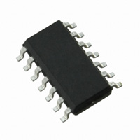
Description The TLE42794G is a monolithic integrated low dropout voltage regulator, especially designed for automotive applications. An input voltage up to 45 V is regulated to an output voltage of 5.0 V. The component is able to drive loads up to 150 mA. It is short-circuit protected by the implemented current limitation and has an integrated overtemperature shutdown. A reset signal is generated for an output voltage VQ,rt of typically 4.65 V. This threshold can be decreased by an external resistor divider. The power-on reset delay time can be programmed by the external delay capacitor. The additional sense comparator provides an early warning function: Any voltage (e.g. the input voltage) can be monitored, an under-voltage condition is indicated by setting the comparator’s output to low. If pull-up resistors are desired at the outputs of the reset and the sense comparator, the TLE42694 with integrated pull-up reistors can be used instead of the TLE42794. PG-DSO-14
PG-SSOP-14 exposed pad
Type TLE42794G TLE42794GM TLE42794E Data Sheet
Package PG-DSO-8 PG-DSO-14 PG-SSOP-14 exposed pad 2
Marking 42794G 42794GM 42794E Rev. 1.1, 2008-10-09
�TLE42794
Overview Dimensioning Information on External Components The input capacitor CI is recommended for compensation of line influences. The output capacitor CQ is necessary for the stability of the control loop. Circuit Description The control amplifier compares a reference voltage to a voltage that is proportional to the output voltage and drives the base of the series transistor via a buffer. Saturation control as a function of the load current prevents any oversaturation of the power element. The component also has a number of internal circuits for protection against: • • • Overload Overtemperature Reverse polarity
Data Sheet
3
Rev. 1.1, 2008-10-09
�TLE42794
Block Diagram
2
Block Diagram
Ι Error Amplifier Reference Current and Saturation Control
Q
Trimming
D
RO
& Reference SO RADJ SI
GND
AEB01955
Figure 1
Block Diagram
Data Sheet
4
Rev. 1.1, 2008-10-09
�TLE42794
Pin Configuration
3
3.1
Pin Configuration
Pin Assignment TLE42794G (PG-DSO-8)
Ι SΙ RADJ D
1 2 3 4
8 7 6 5
AEP01668
Q SO RO GND
Figure 2
Pin Configuration (top view)
3.2
Pin 1
Pin Definitions and Functions TLE42794G (PG-DSO-8)
Symbol I Function Input for compensating line influences, a capacitor to GND close to the IC terminals is recommended Sense Input connect the voltage to be monitored; connect to Q if the sense comparator is not needed Reset Threshold Adjust connect an external voltage divider to adjust reset threshold; connect to GND for using internal threshold Reset Delay Timing connect a ceramic capacitor to GND for adjusting the reset delay time; leave open if the reset function is not needed Ground Reset Output open collector output; external pull-up resistor required, respecting values given in Item 5.6.5; leave open if the reset function is not needed Sense Output open collector output; external pull-up resistor required, respecting values given in Item 5.8.6; leave open if the sense comparator is not needed Output block to GND with a capacitor close to the IC terminals, respecting the values given for its capacitance CQ and ESR in “Functional Range” on Page 9
2
SI
3
RADJ
4
D
5 6
GND
RO
7
SO
8
Q
Data Sheet
5
Rev. 1.1, 2008-10-09
�TLE42794
Pin Configuration
3.3
Pin Assignment TLE42794GM (PG-DSO-14)
RADJ D GND GND GND GND RO
1 2 3 4 5 6 7
14 13 12 11 10 9 8
AEP02248
SI Ι GND GND GND Q SO
Figure 3
Pin Configuration (top view)
3.4
Table 1 Pin 1
Pin Definitions and Functions TLE42794GM (PG-DSO-14)
Symbol
Function Reset Threshold Adjust connect an external voltage divider to adjust reset threshold; connect to GND for using internal threshold Reset Delay Timing connect a ceramic capacitor to GND for adjusting the reset delay time; leave open if the reset function is not needed Ground connect all pins to PCB and heatsink area Reset Output open collector output; external pull-up resistor required, respecting values given in Item 5.6.5; leave open if the reset function is not needed Sense Output open collector output; external pull-up resistor required, respecting values given in Item 5.8.6; leave open if the sense comparator is not needed Output block to GND with a capacitor close to the IC terminals, respecting the values given for its capacitance CQ and ESR in the table “Functional Range” on Page 9 Ground connect all pins to PCB and heatsink area Input for compensating line influences, a capacitor to GND close to the IC terminals is recommended Sense Input connect the voltage to be monitored; connect to Q if the sense comparator is not needed
RADJ
2
D
3, 4, 5, 6 7
GND
RO
8
SO
9
Q
10, 11, 12 GND 13 I
14
SI
Data Sheet
6
Rev. 1.1, 2008-10-09
�TLE42794
Pin Configuration
3.5
Pin Assignment TLE42794E (PG-SSOP-14 exposed pad)
Figure 4
Pin Configuration (top view)
3.6
Table 2 Pin 1
Pin Definitions and Functions TLE42794E (PG-SSOP-14 exposed pad)
Symbol
Function Reset Threshold Adjust connect an external voltage divider to adjust reset threshold; connect to GND for using internal threshold not connected Reset Delay Timing connect a ceramic capacitor to GND for adjusting the reset delay time; leave open if the reset function is not needed Ground connect all pins to PCB and heatsink area Reset Output open collector output; external pull-up resistor required, respecting values given in Item 5.6.4; leave open if the reset function is not needed Sense Output open collector output; external pull-up resistor required, respecting values given in Item 5.8.6; leave open if the sense comparator is not needed not connected Output block to GND with a capacitor close to the IC terminals, respecting the values given for its capacitance CQ and ESR in the table “Functional Range” on Page 9 Input for compensating line influences, a capacitor to GND close to the IC terminals is recommended Sense Input connect the voltage to be monitored; connect to Q if the sense comparator is not needed
RADJ
2, 5, 6 3
n.c.
D
4 7
GND
RO
8
SO
9, 10, 12 11
n.c. Q
13
I
14
SI
Data Sheet
7
Rev. 1.1, 2008-10-09
�TLE42794
General Product Characteristics
4
4.1
General Product Characteristics
Absolute Maximum Ratings
Absolute Maximum Ratings 1) -40 °C ≤ Tj ≤ 150 °C; all voltages with respect to ground, positive current flowing into pin (unless otherwise specified) Pos. Parameter Symbol Limit Values Min. Input, Sense Input 4.1.1 4.1.2 4.1.3 4.1.4 4.1.5 4.1.6 4.1.7 4.1.8 Voltage Voltage Voltage Junction Temperature Storage Temperature ESD Absorption Max. 45 7 7 150 150 2 500 750 V V V °C °C kV V V – – – – – Human Body Model (HBM)2) Charge Device Model (CDM)3) Charge Device Model (CDM)3) at corner pins Unit Conditions
VI VQ VD Tj Tstg VESD,HBM VESD,CDM
-40 -0.3 -0.3 -40 -50 -2 -500 -750
Output, Reset Output, Sense Output Reset Delay, Reset Threshold Temperature
ESD Absorption
1) not subject to production test, specified by design 2) ESD susceptibility Human Body Model “HBM” according to AEC-Q100-002 - JESD22-A114 3) ESD susceptibility Charged Device Model “CDM” according to ESDA STM5.3.1
Note: Stresses above the ones listed here may cause permanent damage to the device. Exposure to absolute maximum rating conditions for extended periods may affect device reliability. Note: Integrated protection functions are designed to prevent IC destruction under fault conditions described in the data sheet. Fault conditions are considered as “outside” normal operating range. Protection functions are not designed for continuous repetitive operation.
Data Sheet
8
Rev. 1.1, 2008-10-09
�TLE42794
General Product Characteristics
4.2
Pos. 4.2.1 4.2.2 4.2.3
Functional Range
Parameter Input Voltage Output Capacitor’s Requirements for Stability Junction Temperature Symbol Min. Limit Values Max. 45 – 3 150 V µF Ω °C – –1) –2) – 5.5 10 – -40 Unit Conditions
VI CQ ESR(CQ) Tj
1) the minimum output capacitance requirement is applicable for a worst case capacitance tolerance of 30% 2) relevant ESR value at f = 10 kHz
Note: Within the functional range the IC operates as described in the circuit description. The electrical characteristics are specified within the conditions given in the related electrical characteristics table.
Data Sheet
9
Rev. 1.1, 2008-10-09
�TLE42794
General Product Characteristics
4.3
Pos.
Thermal Resistance
Parameter Symbol Limit Value Min. Typ. 80 113 172 142 136 Max. – – – – – K/W K/W K/W K/W K/W measured to pin 5
2)
Unit
Conditions
TLE42794G (PG-DSO-8) 4.3.4 4.3.5 4.3.6 4.3.7 4.3.8 TLE42794GM (PG-DSO-14) 4.3.9 4.3.10 4.3.11 4.3.12 4.3.13 TLE42794E (PG-SSOP-14 exposed pad) 4.3.14 4.3.15 4.3.16 4.3.17 4.3.18 Junction to Case1) Junction to Ambient1) Junction to Soldering Point1) Junction to Ambient1) Junction to Soldering Point1) Junction to Ambient
1)
RthJSP RthJA
– – – – –
Footprint only3) 300mm2 heatsink area on PCB3) 600mm2 heatsink area on PCB3) measured to group of pins 3, 4, 5, 10, 11, 12
2)
RthJSP RthJA
– – – – –
27 63 104 73 65
– – – – –
K/W K/W K/W K/W K/W
Footprint only3) 300mm2 heatsink area on PCB3) 600mm2 heatsink area on PCB3) measured to Exposed Pad
2)
RthJC RthJA
– – – – –
10 47 145 63 53
– – – – –
K/W K/W K/W K/W K/W
Footprint only3) 300mm2 heatsink area on PCB3) 600mm2 heatsink area on PCB3)
1) not subject to production test, specified by design 2) Specified RthJA value is according to Jedec JESD51-2,-5,-7 at natural convection on FR4 2s2p board; The Product (Chip+Package) was simulated on a 76.2 x 114.3 x 1.5 mm³ board with 2 inner copper layers (2 x 70µm Cu, 2 x 35µm Cu). Where applicable a thermal via array under the exposed pad contacted the first inner copper layer. 3) Specified RthJA value is according to JEDEC JESD 51-3 at natural convection on FR4 1s0p board; The Product (Chip+Package) was simulated on a 76.2 × 114.3 × 1.5 mm3 board with 1 copper layer (1 x 70µm Cu).
Data Sheet
10
Rev. 1.1, 2008-10-09
�TLE42794
Block Description and Electrical Characteristics
5
5.1
Block Description and Electrical Characteristics
Voltage Regulator
The output voltage VQ is controlled by comparing a portion of it to an internal reference and driving a PNP pass transistor accordingly. The control loop stability depends on the output capacitor CQ, the load current, the chip temperature and the poles/zeros introduced by the integrated circuit. To ensure stable operation, the output capacitor’s capacitance and its equivalent series resistor ESR requirements given in the table “Functional Range” on Page 9 have to be maintained. For details see also the typical performance graph “Output Capacitor Series Resistor ESR(CQ) versus Output Current IQ” on Page 14. As the output capacitor also has to buffer load steps it should be sized according to the application’s needs. An input capacitor CI is strongly recommended to compensate line influences. Connect the capacitors close to the component’s terminals. A protection circuitry prevent the IC as well as the application from destruction in case of catastrophic events. These safeguards contain an output current limitation, a reverse polarity protection as well as a thermal shutdown in case of overtemperature. In order to avoid excessive power dissipation that could never be handled by the pass element and the package, the maximum output current is decreased at input voltages above VI = 22 V. The thermal shutdown circuit prevents the IC from immediate destruction under fault conditions (e.g. output continuously short-circuited) by switching off the power stage. After the chip has cooled down, the regulator restarts. This leads to an oscillatory behaviour of the output voltage until the fault is removed. However, junction temperatures above 150 °C are outside the maximum ratings and therefore significantly reduce the IC’s lifetime. The TLE42794 allows a negative supply voltage. In this fault condition, small currents are flowing into the IC, increasing its junction temperature. This has to be considered for the thermal design, respecting that the thermal protection circuit is not operating during reverse polarity conditions.
Supply
II
I
Q
IQ
Regulated Output Voltage
Saturation Control Current Limitation C CI Temperature S hutdown Bandgap Reference E SR
}
CQ
LOAD
BlockDiagram_VoltageRegulator.vsd
GND
Figure 5
Voltage Regulator
Data Sheet
11
Rev. 1.1, 2008-10-09
�TLE42794
Block Description and Electrical Characteristics
5.2
Electrical Characteristics Voltage Regulator
Electrical Characteristics Voltage Regulator
VI = 13.5 V, -40 °C ≤ Tj ≤150 °C, all voltages with respect to ground, positive current flowing into pin
(unless otherwise specified) Pos. 5.2.1 5.2.2 5.2.3 5.2.4 5.2.5 5.2.6 5.2.7 5.2.8 Parameter Output Voltage Output Current Limitation Load Regulation steady-state Line Regulation steady-state Dropout Voltage1) Symbol Min. Limit Values Typ. 5.0 200 -15 10 250 – 15 70 Max. 5.1 500 – 40 500 200 – – V mA mV mV mV °C °C dB 100 µA < IQ < 100 mA 6 V < VI < 18 V 4.9 150 -30 – – 151 – – Unit Conditions
VQ IQ,max ∆VQ,load ∆VQ,line Vdr Tj,sd Tj,sdh PSRR
Vdr = VI - VQ
Overtemperature Shutdown Threshold Overtemperature Shutdown Threshold Hysteresis Power Supply Ripple Rejection2)
VQ = 4.8V IQ = 5 mA to 100 mA VI = 6 V VI = 6 V to 32 V IQ = 5 mA IQ = 100 mA Tj increasing2) Tj decreasing2)
fripple = 100 Hz Vripple = 0.5 Vpp 1) measured when the output voltage VQ has dropped 100mV from the nominal value obtained at VI = 13.5V
2) not subject to production test, specified by design
Data Sheet
12
Rev. 1.1, 2008-10-09
�TLE42794
Block Description and Electrical Characteristics
5.3
Typical Performance Characteristics Voltage Regulator
Output Current IQ versus Input Voltage VI
01_VQ_TJ.VSD
Output Voltage VQ versus Junction Temperature TJ
5,2 5,1 5
300
02_IQ_VI.VSD
V Q = 4.8 V
I Q = 5 mA V I = 13.5 V
250 200 150 100 50 0
T j = -40 °C T j = 25 °C
V
Q
4,9 4,8 4,7 4,6 -40 0 40 80 120 160
I Q,max [mA]
[V]
T j = 150 °C
0
10
20
30
40
T j [°C]
Power Supply Ripple Rejection PSRR versus ripple frequency fr
90 80 70
03_PSRR_FR.VSD
V I [V]
Line Regulation ∆VQ,line versus Input Voltage VI
4,5 4 3,5
04_DVQ_DVI.VSD
I Q = 5 mA
T j = 150 °C
P S RR [d B ]
[ mV]
60 50 40 30 20 10
T j = 25 °C I Q = 10 mA C Q = 10 µF ceramic
3 2,5 2 1,5 1 0,5 0
T j = 25 °C
∆VQ
T j = -40 °C
0 0,01
0,1
1
10
100
1000
0
10
20
30
40
f [kHz]
V I [V]
Data Sheet
13
Rev. 1.1, 2008-10-09
�TLE42794
Block Description and Electrical Characteristics
Load Regulation ∆VQ,load versus Output Current IQ
0 -2 -4
05_DVQ_DIQ.VSD
Output Capacitor Series Resistor ESR(CQ) versus Output Current IQ
100
06_ESR_IQ.VSD
VI = 13.5 V
10
C Q = 10 µF V I = 13.5 V
-6 -8 -10 -12 -14 0
∆VQ
T j = -40 T j = 25 °C T j = 150
ESR(C Q ) [Ω ]
Unstable Region
[mV]
1
0,1
Stable Region
0,01
20 40 60 80 100
0
50
100
150
I Q [mA]
Dropout Voltage Vdr versus Output Current IQ
300
07_VDR_IQ.VSD
IQ [mA]
Dropout Voltage Vdr versus Junction Temperature Ti
300
08_VDR_TJ.VSD
I Q = 100 mA
250
T j = 150 °C T j = 25 °C
250
200
V DR [mV]
V DR [mV]
T j = -40 °C
200
150 100
150 100
I Q = 25 mA
50
50
I Q = 5 mA I Q = 100 µA
0 0 20 40 60 80 100
0 -40 0 40 80 120 160
I Q [mA]
T j [°C]
Data Sheet
14
Rev. 1.1, 2008-10-09
�TLE42794
Block Description and Electrical Characteristics
5.4
Current Consumption
Electrical Characteristics Voltage Regulator VI = 13.5 V, -40 °C ≤ Tj ≤150 °C, all voltages with respect to ground, positive current flowing into pin (unless otherwise specified) Pos. 5.4.1 5.4.2 5.4.3 5.4.4 Parameter Current Consumption Symbol Min. Limit Values Typ. 210 240 0.7 3.5 Max. 280 300 1 8 µA µA mA mA – – – – Unit Conditions
Iq = IQ - II
Iq
IQ = 100 µA Tj = 25 °C IQ = 100 µA Tj ≤ 85 °C IQ = 10 mA IQ = 50 mA
Data Sheet
15
Rev. 1.1, 2008-10-09
�TLE42794
Block Description and Electrical Characteristics
5.5
Typical Performance Characteristics Current Consumption
Current Consumption Iq versus Output Current IQ
09_IQ_IQ_IQLOW.VSD
Current Consumption Iq versus Output Current IQ (IQ low)
1,6 1,4 1,2
12 10 8
10_IQ_IQ.VSD
V I = 13.5 V T j = 25 °C
V I = 13.5 V T j = 25 °C
I q [mA]
0,8 0,6 0,4 0,2 0 0 5 10 15 20 25
I q [ mA]
1
6 4 2 0 0 20 40 60 80 100 120
I Q [mA]
Current Consumption Iq versus Input Voltage VI
6
11_IQ_VI.VSD
I Q [mA]
5
4
I q [mA]
R LOAD = 100 Ω
3
2
1
R LOAD = 50 k Ω
0 0 10 20 30 40
V I [V]
Data Sheet
16
Rev. 1.1, 2008-10-09
�TLE42794
Block Description and Electrical Characteristics
5.6
Reset Function
The reset function provides several features:
Output Undervoltage Reset: An output undervoltage condition is indicated by setting the Reset Output RO to “low”. This signal might be used to reset a microcontroller during low supply voltage.
Power-On Reset Delay Time: The power-on reset delay time trd allows a microcontoller and oscillator to start up. This delay time is the time frame from exceeding the reset switching threshold VRT until the reset is released by switching the reset output “RO” from “low” to “high”. The power-on reset delay time trd is defined by an external delay capacitor CD connected to pin D charged by the delay capacitor charge current ID,ch starting from VD = 0 V. If the application needs a power-on reset delay time trd different from the value given in Item 5.6.7, the delay capacitor’s value can be derived from the specified values in Item 5.6.7 and the desired power-on delay time:
t rd, new C D = ---------------- × 47nF t rd
with • • •
CD: capacitance of the delay capacitor to be chosen trd,new: desired power-on reset delay time trd: power-on reset delay time specified in this datasheet
For a precise calculation also take the delay capacitor’s tolerance into consideration.
Reset Reaction Time: The reset reaction time avoids that short undervoltage spikes trigger an unwanted reset “low” signal. The reset reaction rime trr considers the internal reaction time trr,int and the discharge time trr,d defined by the external delay capacitor CD (see typical performance graph for details). Hence, the total reset reaction time becomes:
t rr = t rd, int + t rr, d
with • • •
trr: reset reaction time trr,int: internal reset reaction time trr,d: reset discharge
Data Sheet
17
Rev. 1.1, 2008-10-09
�TLE42794
Block Description and Electrical Characteristics Reset Output Pull-Up Resistor RRO: The Reset Output RO is an open collector output requiring an external pull-up resistor. In Table “Electrical Characteristics Reset Function” on Page 20 a minimum value for the external resistor RRO is given. Keep in mind to stay within the values specified for the Reset Output RO in Table 4.1 “Absolute Maximum Ratings” on Page 8 Reset Adjust Function The undervoltage reset switching threshold can be adjusted according to the application’s needs by connecting an external voltage divider (RADJ1, RADJ2) at pin RADJ. For selecting the default threshold connect pin RADJ to GND. When dimensioning the voltage divider, take into consideration that there will be an additional current constantly flowing through the resistors. With a voltage divider connected, the reset switching threshold VRT,new is calculated as follows:
R ADJ, 1 + R ADJ, 2 V RT, new = ----------------------------------------- × V RADJ, th R ADJ, 2
with • • •
VRT,new: the desired new reset switching threshold RADJ1, RADJ2: resistors of the external voltage divider VRADJ,th: reset adjust switching threshold given in Table “Electrical Characteristics Reset Function” on Page 20
Supply
I
Q
VDD
Int. Supply Control
CQ ID,ch
RO
RRO
Reset
VRADJ,th
OR
VDST
I RO RADJ,1
MicroController
ID,dch
RADJ optional
I RADJ
GND
BlockDiagram_ResetAdjust.vsd
D
RADJ,2 CD
GND
Figure 6
Block Diagram Reset Function
Data Sheet
18
Rev. 1.1, 2008-10-09
�TLE42794
Block Description and Electrical Characteristics
VI
t VQ VRT t < trr,total
1V
t VD V DU V DRL t VRO t rd trr,total trd t rr,total t rd t rr,total t rd
V RO,low
1V
t
Thermal Shutdown Input Voltage Dip Undervoltage Spike at output Overload
T i mi n g Di a g ra m_ Re se t . vs
Figure 7
Timing Diagram Reset
Data Sheet
19
Rev. 1.1, 2008-10-09
�TLE42794
Block Description and Electrical Characteristics
Electrical Characteristics Reset Function
VI = 13.5 V, -40 °C ≤ Tj ≤ 150 °C, all voltages with respect to ground, positive current flowing into pin
(unless otherwise specified) Pos. Parameter Symbol Min. Output Undervoltage Reset 5.6.1 Default Output Undervoltage Reset VRT Switching Thresholds Reset Adjust Switching Threshold Reset Adjustment Range1) Reset Output Low Voltage 4.5 4.65 4.8 V Limit Values Typ. Max. Unit Conditions
VQ decreasing
Output Undervoltage Reset Threshold Adjustment 5.6.2 5.6.3 5.6.4
VRADJ,th VRT,range VRO,low
1.26 3.50 –
1.35 – 0.1
1.44 4.65 0.4
V V V
3.5 V ≤ VQ < 5 V – 1 V ≤ VQ ≤ VRT external RRO,ext = 10 kΩ 1 V ≤ VQ ≤ VRT ; VRO ≤ 0.4 V –
Reset Output RO
5.6.5
Reset Output External Pull-up Resistor to VQ Delay Pin Output Voltage Power On Reset Delay Time Upper Delay Switching Threshold Lower Delay Switching Threshold Delay Capacitor Charge Current Delay Capacitor Reset Discharge Current Delay Capacitor Discharge Time
RRO,ext
10
–
–
kΩ
Reset Delay Timing 5.6.6 5.6.7 5.6.8 5.6.9 5.6.10 5.6.11 5.6.12
VD trd VDU VDL ID,ch ID,dch trr,d
– 17 – – – – –
– 28 1.8 0.45 6.5 70 1.9
5 39 – – – – 3
V ms V V µA mA µs
CD = 100 nF
– –
VD = 1 V VD = 1 V
Calculated Value:
5.6.13 5.6.14
Internal Reset Reaction Time Reset Reaction Time
trr,int trr,total
– –
3 4.9
7 10
µs µs
trr,d = CD*(VDU VDL)/ ID,dch CD = 100 nF CD = 0 nF 2)
Calculated Value: trr,total = trr,int + trr,d CD = 100 nF
1) VRT is scaled linearly, in case the Reset Switching Threshold is modified 2) parameter not subject to production test; specified by design
Data Sheet
20
Rev. 1.1, 2008-10-09
�TLE42794
Block Description and Electrical Characteristics
5.7
Typical Performance Characteristics Reset
Power On Reset Delay Time trd versus Junction Temperature Tj
35
12_TRD_TJ.VSD
C D = 100 nF
30
25
t rd [ms]
20
15
10
5
0 -40 0 40 80 120 160
T j [°C]
Data Sheet
21
Rev. 1.1, 2008-10-09
�TLE42794
Block Description and Electrical Characteristics
5.8
Early Warning Function
The additional sense comparator provides an early warning function: Any voltage (e.g. the input voltage) can be monitored, an undervoltage condition is indicated by setting the comparator’s output to low.
Sense Input Voltage VSI, High
VSI, Low
t Sense Output High
Low t
AED03049
Figure 8
Sense Timing Diagram
Electrical Characteristics Early Warning Function
VI = 13.5 V, -40 °C ≤ Tj ≤ 150 °C, all voltages with respect to ground, positive current flowing into pin
(unless otherwise specified) Pos. Parameter Symbol Min. Sense Comparator Input 5.8.1 5.8.2 5.8.3 5.8.4 Sense Threshold High Sense Threshold Low Sense Switching Hysteresis Sense Input Current Limit Values Typ. 1.31 1.22 90 -0.1 Max. 1.38 1.28 160 1 V V mV µA – – – – Rev. 1.1, 2008-10-09 Unit Conditions
VSI,high VSI,low VSI,hy ISI
1.24 1.16 20 -1 22
Data Sheet
�TLE42794
Block Description and Electrical Characteristics Electrical Characteristics Early Warning Function
VI = 13.5 V, -40 °C ≤ Tj ≤ 150 °C, all voltages with respect to ground, positive current flowing into pin (unless otherwise specified)
Pos. Parameter Symbol Min. Sense Comparator Output 5.8.5 Sense Output Low Voltage Limit Values Typ. 0.1 Max. 0.4 V Unit Conditions
VSO,low
–
5.8.6
Sense Output External Pull-up Resistor to VQ
RSO,ext
10
–
–
kΩ
VSI < VSI,low VI > 5.5 V RSO,ext = 10 kΩ VI > 5.5 V VSO ≤ 0.4 V
Data Sheet
23
Rev. 1.1, 2008-10-09
�TLE42794
Package Outlines
6
Package Outlines
0.35 x 45˚
1.75 MAX.
0.175 ±0.07 (1.45)
4 -0.21)
0.19 +0.06
C
1.27 0.41+0.1 2) -0.06 0.2
M
0.1 A B 8x
B 6 ±0.2
0.64 ±0.25 0.2
M
8 MAX.
C 8x
GPS01181
Rev. 1.1, 2008-10-09
8
5
1
4
5 -0.2 1) Index Marking
A
1) Does not include plastic or metal protrusion of 0.15 max. per side 2) Lead width can be 0.61 max. in dambar area
Figure 9
PG-DSO-8
Data Sheet
24
�TLE42794
Package Outlines
0.35 x 45˚
1.75 MAX.
0.175 ±0.07 (1.47)
C
4 -0.2
1.27 0.41+0.10 2) -0.06 14
B
0.1
0.2 M A B 14x
8 6±0.2
0.64 ±0.25
0.2 M C
1 7 1) 8.75 -0.2
A
Index Marking 1) Does not include plastic or metal protrusion of 0.15 max. per side 2) Lead width can be 0.61 max. in dambar area GPS01230
Figure 10
PG-DSO-14
Data Sheet
25
Rev. 1.1, 2008-10-09
8˚MAX.
1)
0.19 +0.06
�TLE42794
Package Outlines
0.35 x 45˚
Stand Off (1.45)
1.7 MAX.
3.9 ±0.11)
0.1 C D
0 ... 0.1
0.19 +0.06
0.08 C 6 ±0.2
0.65 0.25 ±0.05 2)
C
0.64 ±0.25
D 0.2
8˚ MAX.
M
0.15 M C A-B D 14x
D 8x
A
14 8
Bottom View 3 ±0.2
1 7
1
7
B 0.1 C A-B 2x
Exposed Diepad
14
8
4.9 ±0.11)
Index Marking
1) Does not include plastic or metal protrusion of 0.15 max. per side 2) Does not include dambar protrusion
PG-SSOP-14-1,-2,-3-PO V02
Figure 11
PG-SSOP-14 exposed pad
Green Product (RoHS compliant) To meet the world-wide customer requirements for environmentally friendly products and to be compliant with government regulations the device is available as a green product. Green products are RoHS-Compliant (i.e Pb-free finish on leads and suitable for Pb-free soldering according to IPC/JEDEC J-STD-020).
For further information on alternative packages, please visit our website: http://www.infineon.com/packages. Data Sheet 26
2.65 ±0.2
Dimensions in mm Rev. 1.1, 2008-10-09
�TLE42794
Revision History
7
Revision 1.1
Revision History
Date 2008-10-09 Changes package version TLE42794E in PG-SSOP-14 exposed pad and all related information added In “Overview” on Page 2 package graphic for PG-SSOP-14 exposed pad and product name “TLE42794E” added In Chapter 3 “Pin Assignment TLE42794E (PG-SSOP-14 exposed pad)” on Page 7 and “Pin Definitions and Functions TLE42794E (PG-SSOP-14 exposed pad)” on Page 7 added In “Thermal Resistance” on Page 10 values for TLE42794E added In “Package Outlines” on Page 24 outlines for TLE4279E added
1.0
2008-09-19
initial version data sheet
Data Sheet
27
Rev. 1.1, 2008-10-09
�Edition 2008-10-09 Published by Infineon Technologies AG 81726 Munich, Germany © 2008 Infineon Technologies AG All Rights Reserved. Legal Disclaimer The information given in this document shall in no event be regarded as a guarantee of conditions or characteristics. With respect to any examples or hints given herein, any typical values stated herein and/or any information regarding the application of the device, Infineon Technologies hereby disclaims any and all warranties and liabilities of any kind, including without limitation, warranties of non-infringement of intellectual property rights of any third party. Information For further information on technology, delivery terms and conditions and prices, please contact the nearest Infineon Technologies Office (www.infineon.com). Warnings Due to technical requirements, components may contain dangerous substances. For information on the types in question, please contact the nearest Infineon Technologies Office. Infineon Technologies components may be used in life-support devices or systems only with the express written approval of Infineon Technologies, if a failure of such components can reasonably be expected to cause the failure of that life-support device or system or to affect the safety or effectiveness of that device or system. Life support devices or systems are intended to be implanted in the human body or to support and/or maintain and sustain and/or protect human life. If they fail, it is reasonable to assume that the health of the user or other persons may be endangered.
�