5-V Voltage Regulator
TLE 4285 G
Features • • • • • • • • • • 15 mA current capability Low quiescent current consumption Power fail output Wide operation range: up to 45 V Wide temperature range: -40 °C to 150 °C Output protected against short circuit Overtemperature protection Very small SMD-Package PG-SCT-595-5 Green product (RohS compliant) AEC qualified
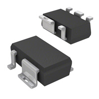
PG-SCT-595-5
Functional Description The TLE 4285 G is a 5-V fixed voltage regulator in a very small SMD package PG-SCT-595-5. The maximum input voltage is 45 V. The output is able to drive an output current of more than 10 mA while it regulates the output voltage within a 4% accuracy. The Power Fail Output (open collector) is switched to low in case of under-voltage at the output pin. To reduce external components the Power Fail Output has an internal pull-up resistor of 50 kΩ which is connected to the output Q. The device incorporates a temperature protection that disables the circuit at overtemperature.
Type TLE 4285 G
Data Sheet
Package PG-SCT-595-5
1
Marking B1
Rev. 2.2, 2008-04-21
�TLE 4285 G
PG-SCT-595-5
PF
1 5 GND
GND
2
Ι
3
4
Q
AEP02279
Figure 1 Table 1 Pin No. 1 2 3 4 5
Pin Configuration (top view) Pin Definitions and Functions Symbol PF GND I Q GND Function Power Fail; L for under-voltage; internally connected to Q via 50 kΩ pull-up resistor Ground; internally connected to pin 5 Input voltage Output voltage; must be blocked by a capacitor
CQ ≥ 1 µF, ESR ≤ 10 Ω to GND
Ground; internally connected to pin 2
Data Sheet
2
Rev. 2.2, 2008-04-21
�TLE 4285 G
Functional Block Diagram
Protection Ι 3 4 Q
Reference
Regulator
Power Fail Control
1
PF
2, 5 GND
AEB02186
Figure 2
Block Diagram
Data Sheet
3
Rev. 2.2, 2008-04-21
�TLE 4285 G
Table 2
Absolute Maximum Ratings
-40 °C < Tj < 150 °C Parameter Input Voltage Current Output Voltage Current Power Fail Voltage Current Temperatures Junction temperature Storage temperature Thermal Resistances Junction pin Junction ambient Symbol Limit Values Min. Max. 45 * 16 * 45 * 150 150 30 55 V mA V mA V µA °C °C K/W K/W – * internally limited – * internally limited – * internally limited – – measured to pin 5
1)
Unit
Remarks
VI II VQ IQ VPF IPF Tj Tstg Rthj-pin Rthj-a
-0.3 -20 -0.3 -20 -0.3 -500 -40 -50 – –
1) Package mounted on PCB 40 × 40 × 1.5 mm3/6 cm2 Cu.
Note: Maximum ratings are absolute ratings; exceeding any one of these values may cause irreversible damage to the integrated circuit. Table 3 Parameter Input voltage Output current Junction temperature Operating Range Symbol Limit Values Min. Max. 42 – 150 V mA °C – – – 6 15 -40 Unit Remarks
VI IQ Tj
Data Sheet
4
Rev. 2.2, 2008-04-21
�TLE 4285 G
Table 4
Electrical Characteristics
6.2 V < VI < 36 V; -40 °C < Tj < 150 °C; unless otherwise specified Parameter Output Output voltage Output voltage Drop voltage Output capacitor Output current Current Consumption Quiescent current Symbol Min. Limit Values Typ. 5.0 5.0 0.8 – – 100 Max. 5.15 5.20 1.1 – 70 150 V V V µF mA µA Unit Test Condition
VQ VQ Vdr CQ IQ Iq
4.85 4.8 0.6 1 15 –
Tj = 25 °C; 1 mA < IQ < 10 mA 1 mA < IQ < 10 mA IQ = 10 mA1)
ESR ≤ 10 Ω at 10 kHz –
IQ < 10 mA; VI = 13.5 V
0 mA < IQ
很抱歉,暂时无法提供与“TLE4285G”相匹配的价格&库存,您可以联系我们找货
免费人工找货