1. 物料型号:
- 型号:TLE 4921-3U
- 订货代码:Q67006-A9171
2. 器件简介:
- TLE 4921-3U是一款双极型IC,具有高级性能,高灵敏度和对称阈值,适用于转速检测和定时应用,如防抱死制动系统、变速器、曲轴等。
3. 引脚分配:
- 1号引脚:VS(供电电压)
- 2号引脚:Q(输出)
- 3号引脚:GND(地)
- 4号引脚:C(电容器)
4. 参数特性:
- 供电电压:4.5V至24V
- 接点温度范围:-40°C至170°C
- 预感应磁场强度:-500 mT至500 mT
- 差分感应:-80 mT至80 mT
5. 功能详解:
- TLE 4921-3U通过测量磁场的差分磁通密度来检测铁磁和永磁结构的运动和位置。
- 使用外部电容器,通过具有低截止频率的有源高通滤波器缓慢调整产生的霍尔电压信号。
- TLE 4921-3U可以在恶劣环境下检测齿轮轮旋转,对齿轮轮的冲击和波动没有影响。
6. 应用信息:
- 适用于铁磁齿轮应用,需要通过永磁体(例如SmCo5)的南极或北极对IC进行偏置。
- 最大气隙取决于所用磁体的磁场强度和齿轮的尺寸、材料等。
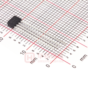
7. 封装信息:
- 封装类型:P-SSO-4-1(塑料单小外形封装)
- 芯片到IC上表面的距离:0.3 mm