D ata Sheet, V 1.1, January 2008
TLE4921-5U
Dynamic Differential Hall Effect Sensor IC
Sensors
Never
stop
thinking.
�Edition 2008-01 Published by Infineon Technologies AG, St.-Martin-Strasse 53, 81669 München, Germany
© Infineon Technologies AG 2008. All Rights Reserved.
Attention please! The information herein is given to describe certain components and shall not be considered as a guarantee of characteristics. Terms of delivery and rights to technical change reserved. We hereby disclaim any and all warranties, including but not limited to warranties of non-infringement, regarding circuits, descriptions and charts stated herein. Information For further information on technology, delivery terms and conditions and prices please contact your nearest Infineon Technologies Office (www.infineon.com). Warnings Due to technical requirements components may contain dangerous substances. For information on the types in question please contact your nearest Infineon Technologies Office. Infineon Technologies Components may only be used in life-support devices or systems with the express written approval of Infineon Technologies, if a failure of such components can reasonably be expected to cause the failure of that life-support device or system, or to affect the safety or effectiveness of that device or system. Life support devices or systems are intended to be implanted in the human body, or to support and/or maintain and sustain and/or protect human life. If they fail, it is reasonable to assume that the health of the user or other persons may be endangered.
�TLE4921-5U Revision History: Previous Version: Page 5 11 20 21 2008-01 V1.0 V 1.1
Subjects (major changes since last revision) Ordering Code changed “Output leakage current” unit corrected Figures “Delay Time between Switching Threshold” exchanged and corrected Figure “Delay Time versus Differential Field” corrected
We Listen to Your Comments Any information within this document that you feel is wrong, unclear or missing at all? Your feedback will help us to continuously improve the quality of this document. Please send your proposal (including a reference to this document) to: sensors@infineon.com
Template: mc_a5_ds_tmplt.fm / 4 / 2004-09-15
�TLE4921-5U
Table of Contents 1 1.1 1.2 2 2.1 2.2 2.3 3 4 5 6 7 8
Page
Overview . . . . . . . . . . . . . . . . . . . . . . . . . . . . . . . . . . . . . . . . . . . . . . . . . . . 5 Features . . . . . . . . . . . . . . . . . . . . . . . . . . . . . . . . . . . . . . . . . . . . . . . . . . . . 5 Pin Configuration (view on branded side of component) . . . . . . . . . . . . . . . . . . . . . . . . . . . . . 6 General . . . . . . . . . . . . . . . . . . . . . . . . . . . . . . . . . . . . . . . . . . . . . . . . . . . . Block Diagram . . . . . . . . . . . . . . . . . . . . . . . . . . . . . . . . . . . . . . . . . . . . . . . Functional Description . . . . . . . . . . . . . . . . . . . . . . . . . . . . . . . . . . . . . . . . . Circuit Description (see Figure 2) . . . . . . . . . . . . . . . . . . . . . . . . . . . . . . . . 7 7 8 8
Maximum Ratings . . . . . . . . . . . . . . . . . . . . . . . . . . . . . . . . . . . . . . . . . . . 9 Operating Range . . . . . . . . . . . . . . . . . . . . . . . . . . . . . . . . . . . . . . . . . . . 10 Electrical and Magnetic Parameters . . . . . . . . . . . . . . . . . . . . . . . . . . . 11 Application Configurations . . . . . . . . . . . . . . . . . . . . . . . . . . . . . . . . . . . 14 Typical Performance Characteristics . . . . . . . . . . . . . . . . . . . . . . . . . . 18 Package Outlines . . . . . . . . . . . . . . . . . . . . . . . . . . . . . . . . . . . . . . . . . . . 25
Data Sheet
4
V 1.1, 2008-01
�Dynamic Differential Hall Effect Sensor IC
TLE4921-5U
Bipolar IC
1
1.1
• • • • • • • • • • • • • • •
Overview
Features
Advanced performance High sensitivity Symmetrical thresholds High piezo resistivity Reduced power consumption South and north pole pre-induction possible AC coupled Digital output signal Two-wire and three-wire configuration possible Large temperature range Large airgap Low cut-off frequency Protection against overvoltage Protection against reversed polarity Output protection against electrical disturbances
The differential Hall Effect sensor TLE4921-5U provides a high sensitivity and a superior stability over temperature and symmetrical thresholds in order to achieve a stable duty cycle. TLE4921-5U is particularly suitable for rotational speed detection and timing applications of ferromagnetic toothed wheels such as anti-lock braking systems, transmissions, crankshafts, etc. The integrated circuit (based on Hall effect) provides a digital signal output with frequency proportional to the speed of rotation. Unlike other rotational sensors differential Hall ICs are not influenced by radial vibration within the effective airgap of the sensor and require no external signal processing.
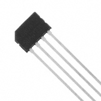
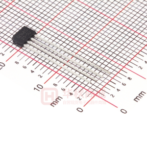
Type TLE4921-5U
Data Sheet
Marking 215U
5
Ordering Code SP000013593
Package PG-SSO-4-1
V 1.1, 2008-01
�TLE4921-5U
Overview
1.2
Pin Configuration (view on branded side of component)
B A
1.53
2.67 2.5
0.2 B
Center of sensitive area 1 2 3 4
0.2 A
VS
Q GND C
AEP01694
Figure 1 Table 1 Pin No. 1 2 3 4 Pin Definitions and Functions Symbol Function Supply voltage Output Ground Capacitor
VS
Q GND
C
Data Sheet
6
V 1.1, 2008-01
�TLE4921-5U
General
2
2.1
General
Block Diagram
VS
1
Protection Device
Internal Reference and Supply
VREG (3V)
Hall-Probes SchmittTrigger Protection Open Collector Device 2
Amplifier
HighpassFilter
Q
3 GND
4 CF
AEB01695
Figure 2
Block Diagram
Data Sheet
7
V 1.1, 2008-01
�TLE4921-5U
General
2.2
Functional Description
The Differential Hall Sensor IC detects the motion and position of ferromagnetic and permanent magnet structures by measuring the differential flux density of the magnetic field. To detect ferromagnetic objects the magnetic field must be provided by a back biasing permanent magnet (south or north pole of the magnet attached to the rear unmarked side of the IC package). Using an external capacitor the generated Hall voltage signal is slowly adjusted via an active high pass filter with a low cut-off frequency. This causes the output to switch into a biased mode after a time constant is elapsed. The time constant is determined by the external capacitor. Filtering avoids ageing and temperature influence from Schmitttrigger input and eliminates device and magnetic offset. The TLE4921-5U can be exploited to detect toothed wheel rotation in a rough environment. Jolts against the toothed wheel and ripple have no influence on the output signal. Furthermore, the TLE4921-5U can be operated in a two-wire as well as in a three-wireconfiguration. The output is logic compatible by high/low levels regarding on and off.
2.3
Circuit Description (see Figure 2)
The TLE4921-5U is comprised of a supply voltage reference, a pair of Hall probes spaced at 2.5 mm, differential amplifier, filter for offset compensation, Schmitt trigger, and an open collector output. The TLE4921-5U was designed to have a wide range of application parameter variations. Differential fields up to ± 80 mT can be detected without influence to the switching performance. The pre-induction field can either come from a magnetic south or north pole, whereby the field strength up to 500 mT or more will not influence the switching points. The improved temperature compensation enables a superior sensitivity and accuracy over the temperature range. Finally the optimized piezo compensation and the integrated dynamic offset compensation enable easy manufacturing and elimination of magnet offsets. Protection is provided at the input/supply (pin 1) for overvoltage and reverse polarity and against over-stress such as load dump, etc., in accordance with ISO-TR 7637 and DIN 40839. The output (pin 2) is protected against voltage peaks and electrical disturbances.
Data Sheet
8
V 1.1, 2008-01
�TLE4921-5U
Maximum Ratings
3
Table 2 Parameter
Maximum Ratings
Absolute Maximum Ratings Tj = -40°C to 150°C Symbol min. Limit Values max. 30 30 50 50 3 150 160 170 210 150 190 °C K/W V V mA mA V °C 5000 h 2500 h 1000 h 40 h -35 1) -0.7 – – -0.3 – – – – Unit Remarks
Supply voltage Output voltage Output current Output reverse current Capacitor voltage Junction temperature
VS VQ IQ -IQ VC Tj
Storage temperature Thermal resistance PG-SSO-4-1
TS RthJA
-40 –
Current through ISZ input-protection device Current through IQZ output-protection device
1) Reverse current < 10 mA
–
200
mA
t < 2 ms; v = 0.1 t < 2 ms; v = 0.1
–
200
mA
Data Sheet
9
V 1.1, 2008-01
�TLE4921-5U
Operating Range
4
Table 3
Operating Range
ESD Protection Human Body Model (HBM) tests according to: Standard EIA/JESD22-A114-B HBM Symbol min. – Limit Values max. ±2 kV Unit Remarks
Parameter
ESD - protection VESD Table 4 Parameter Supply voltage Junction temperature Pre-induction
Operating Range Symbol min. Limit Values typ. – – – – – max. 24 150 160 170 500 mT V °C 5000 h 2500 h 1000 h at Hall probe; independent of magnet orientation 4.5 -40 – – Unit Remarks
VS Tj
B0
∆B
-500
Differential induction
-80
–
80
mT
Note: In the operating range the functions given in the circuit description are fulfilled.
Data Sheet
10
V 1.1, 2008-01
�TLE4921-5U
Electrical and Magnetic Parameters
5
Table 5 Parameter
Electrical and Magnetic Parameters
Electrical Characteristics Symbol min. Limit Values typ. 5.3 5.9 0.25 max. 8.0 8.8 0.6 mA mA V 3.8 4.3 Unit Test Condition Test Circuit 1 1 1
Supply current
IS
Output saturation voltage Output leakage current
VQSAT IQL
–
VQ = high IQ = 0 mA VQ = low IQ = 40 mA IQ = 40 mA VQ = 24 V
-20 mT < ∆B < 20 mT 1) 2) f = 200 Hz
– -1
– 0
50 1
µA mT
1 2
Center of ∆Bm switching points: (∆BOP + ∆BRP) / 2 Operate point Release point Hysteresis ∆BOP ∆BRP ∆BH
– 0 0.5
– – 1.5
0 – 2.5
mT mT mT
f = 200 Hz, ∆B = 20 mT f = 200 Hz, ∆B = 20 mT f = 200 Hz, ∆B = 20 mT
2 2 2
Overvoltage protection at supply voltage VSZ VQZ at output Output rise time Output fall time Delay time
27 27 – – – – – 35
– – – – – – 0 43
35 35 0.5 0.5 25 10 15 52
V V µs µs µs µs µs kΩ
tr tf tdop tdrp tdop - tdrp RC
IS = 16 mA IQ = 16 mA IQ = 40 mA CL = 10 pF IQ = 40 mA CL = 10 pF f = 10 kHz ∆B = 5 mT
25°C ±2°C
1 1 1 1 2
Filter input resistance
1
Data Sheet
11
V 1.1, 2008-01
�TLE4921-5U
Electrical and Magnetic Parameters Table 5 Parameter Filter sensitivity to ∆B Filter bias voltage Frequency Resistivity against mechanical stress (piezo) Electrical Characteristics (cont’d) Symbol min. Limit Values typ. -5 2 – – – max. – 2.4 20000 0.1 0.1 – 1.6
3)
Unit
Test Condition
Test Circuit 1 1 2 2 4)
SC VC f
∆Bm ∆BH
mV/mT – V Hz mT mT ∆B = 0 ∆B = 5 mT F=2N
-0.1 -0.1
1) The Current consumption characteristic will be different and the specified values can slightly change 2) Leakage currents at pin 4 should be avoided. The bias shift of Bm caused by a leakage current IL can be
IL × RC ( T ) calculated by: ∆ B m = ---------------------------SC ( T )
3) For higher ∆B the values may exceed the limits like following | ∆Bm | < | 0.05 × ∆B | 1 4) Depends on filter capacitor CF. The cut-off frequency is given by f = --------------------------------- . The switching points are 2 π × RC × CF guaranteed over the whole frequency range, but amplitude modification and phase shift due to the 1st order highpass filter have to be taken into account.
Note: The listed characteristics are ensured over the operating range of the integrated circuit. Typical characteristics specify mean values expected over the production spread. If not otherwise specified, typical characteristics apply at Tj = 25°C and the given supply voltage.
Data Sheet
12
V 1.1, 2008-01
�TLE4921-5U
Electrical and Magnetic Parameters
RP
300 Ω
VSZ
1
IS VS RL IQ , IQR
VLD
4.7 nF
VS
IC1) 4 C
TLE4921-5U
Q
2
VC
GND 3
VQSAT, VQZ
CL
1)
RC =
∆VC ∆ IC
AES01696
Figure 3
Test Circuit 1
1 VS
1 kΩ 2 f min f max ∆ BOP ∆ BHy
AES01258
VS
4
C
TLE4921-5U
Q
VQ
CF 470 nF
GND 3
Figure 4
Test Circuit 2
Data Sheet
13
V 1.1, 2008-01
�TLE4921-5U
Application Configurations
6
Application Configurations
Two possible applications are shown in Figure 7 and Figure 8 (Toothed and Magnet Wheel). The difference between two-wire and three-wire application is shown in Figure 9. Gear Tooth Sensing In the case of ferromagnetic toothed wheel application the IC has to be biased by the south or north pole of a permanent magnet (e.g. SmCO5 (Vacuumschmelze VX145)) with the dimensions 8 mm × 5 mm × 3 mm) which should cover both Hall probes. The maximum air gap depends on: – the magnetic field strength (magnet used; pre-induction) and – the toothed wheel that is used (dimensions, material, etc.; resulting differential field) a centered distance of Hall probes b Hall probes to IC surface L IC surface to tooth wheel a = 2.5 mm b = 0.3 mm Figure 5 Sensor Spacing Conversion DIN – ASA
N S b L a
AEA01259
T
d
AEA01260
m = 25.4 mm/p T = 25.4 mm CP
ASA diameter (mm) number of teeth module m = d/z (mm) pitch T = π × m (mm) Tooth Wheel Dimensions
DIN
d z m T
Figure 6
p
PD CP
diameter pitch p circular pitch
= z/d (inch)
pitch diameter PD = z/p (inch) CP = 1 inch × π/p
Data Sheet
14
V 1.1, 2008-01
�TLE4921-5U
Application Configurations
Gear Wheel
Hall Sensor 1
Hall Sensor 2
Signal Processing Circuitry
S (N) N (S)
Permanent Magnet
AEA01261
Figure 7
TLE4921-5U, with Ferromagnetic Toothed Wheel
Magnet Wheel
S N
Hall Sensor 1
S
Hall Sensor 2
Signal Processing Circuitry
AEA01262
Figure 8
Data Sheet
TLE4921-5U, with Magnet Wheel
15 V 1.1, 2008-01
�TLE4921-5U
Application Configurations
Two-wire-application Line 1 4 CF 470 nF VS C GND 3 VSIGNAL RS Q 2 RL
VS
Sensor for example : R L = 330 Ω R S = 120 Ω
Mainframe
AES01263
Three-wire-application Rp 1 VS C GND 3 Q Line RL 2 4.7 nF 4.7 nF VSIGNAL
VS
4 CF 470 nF
Sensor for example : R L = 330 Ω R P = 0 ... 330 Ω
Mainframe
AES01264
Figure 9
Application Circuits
Data Sheet
16
V 1.1, 2008-01
�TLE4921-5U
Application Configurations
N (S) S (N) 1 4
B1
Wheel Profile
B2
Missing Tooth
Magnetic Field Difference ∆ B = B2 _ B1 ∆ BRP = 0.75 mT
Small Airgap Large Airgap
∆ BHYS
∆ BOP = _ 0.75 mT
Output Signal VQ
Operate point: B2 _ B1 < ∆ BOP switches the output ON (VQ = LOW) Release point: B2 _ B1 > ∆ BRP switches the output OFF (VQ = HIGH) ∆ BRP = ∆ BOP + ∆ BHYS The magnetic field is defined as positive if the south pole of the magnet shows towards the rear side of the IC housing.
AED01697
Figure 10
System Operation
Data Sheet
17
V 1.1, 2008-01
�TLE4921-5U
Typical Performance Characteristics
7
Typical Performance Characteristics
Quiescent Current versus Temperature
AED03167
AED03168
Quiescent Current versus Supply Voltage
10 mA IS 9 8 7 6 5 4 3 2 1 0 0 5 10 15
I Q = 40 mA
10 mA IS 9 8 7
I ON = 40 mA
IS ON IS OFF
6 5 4 3 2
IS ON IS OFF
IS Diff
20 V 25
1 0 -50 -10 30
IS Diff
70 110 150 ˚C 230
VS
Tj
Quiescent Current versus Output Current
10 mA IS 9 8
AED03169
Saturation Voltage versus Temperature
VQ
400 mV
AED03170
VS = 12 V
VS = 4.5 V I Q = 50 mA
300
7 6 5 4 3
IS ON
250 200 150 100
2 1 0 0 10 20 30 40 mA 50
50 0 -50
0
50
100
150 ˚C 200
I OUT
Data Sheet 18
Tj
V 1.1, 2008-01
�TLE4921-5U
Typical Performance Characteristics Output Saturation Voltage versus IQ @ 25°C Tj
300 mV 200
Out Sat Voltage
AED03171
Saturation Voltage versus Supply Voltage
0.40 V
AED03172
I Q ±50 mA, VS = 4.5 V
VQ
I Q = 40 mA Tj = 25 ˚C
100 0
0.30 0.25 0.20
-100
0.15
-200 -300 -400 -60
0.10 0.05 0
-40
-20
0
20
mA 60
0
5
10
15
20
25
30
IQ
VS
Center of Switching Points versus Temperature
2 mT
AED03173
Hysteresis versus Temperature
AED03174
BM
B M = ( B OP + B RP)/2 f = 200 Hz
B Hy
4 mT
B Hy = B RP - B OP f = 200 Hz
1
max
3 max
0
typ
2 typ
-1
min
1 min
-2 -60
-20
20
60
100
˚C 180
0 -60
-20
20
60
100
˚C 180
Tj
Tj
Data Sheet
19
V 1.1, 2008-01
�TLE4921-5U
Typical Performance Characteristics Minimum Switching Field versus Frequency
1.5 mT
AED03175
Minimum Switching Field versus Frequency
1.5 mT
AED03176
B min
CF = 1 µF
B min
CF = 1 µF
1.0
1.0
Tj = -40 ˚C Tj = 25 ˚C
0.5
0.5
Tj = 170 ˚C Tj = 150 ˚C
0 -2 10
10-1
100
101 kHz 102
0 -2 10
10-1
100
101 kHz 102
f
f
Delay Time between Switching Threshold ∆B and Falling Edge of VOUT at Tj = 25°C
25 µs
Delay Time between Switching Threshold ∆B and Rising Edge of VOUT at Tj = 25°C
25 µs
∆B = 2mT, f =200Hz
∆B = 2mT, f =200Hz
t dop
20
t drp
20
15
15
10
10
∆B = 2mT
5
∆B = 2mT
5
∆B = 5mT
0 0 5000 10000 15000 20000 Hz 25000
∆B = 5mT
0 0 5000 10000 15000 20000 Hz 25000
f
f
Data Sheet
20
V 1.1, 2008-01
�TLE4921-5U
Typical Performance Characteristics Delay Time versus Differential Field Delay Time versus Temperature
8.5 µs 8.0 7.5
AED03180
t
∆ B = 2 mT, f = 200 Hz
tdrp
7.0 6.5 6.0 5.5 5.0 -60
tdop
-10
40
90
140 ˚C 190
T
Rise and Fall Time versus Temperature
AED03181
Rise and Fall Time versus Output Current
120 ns 100
AED03182
t
40 ns 35
I Q = 40 mA
t
Tj = 25 ˚C
30
tr
25
80
60
tf
20
40
tr tf
20
15
10 -50
0
50
100
150 ˚C 200
0
Tj
0
20
40
60
80 mA 100
I OUT
Data Sheet
21
V 1.1, 2008-01
�TLE4921-5U
Typical Performance Characteristics Capacitor Voltage versus Temperature
AED03183
Switching Thresholds versus Mechanical Stress
1.0 ∆ Brp , (∆ Bop ) 0.9
AED03184
VC
3.0 V 2.5 typ 2.0
Tj = 25 ˚C
0.8 max
1.5
min 0.7
1.0
0.5
0.6
0 -50
0
50
100
150 ˚C 200
0.5
0
1
2
3
4N5
Tj
F
Filter Sensitivity versus Temperature
AED03185
Filter Input Resistance versus Temperature
RC R C @ 25˚C
1.6
AED03186
0 mV/mT SC -1 -2 -3 -4 typ -5 -6 -7 -8 -9 -10 -50 0 50 100
1.4 1.3 1.2 1.1 1.0 0.9 0.8 0.7
150 ˚C 200
0.6 -50
0
50
100
150 ˚C 200
Tj
Tj
Data Sheet
22
V 1.1, 2008-01
�TLE4921-5U
Typical Performance Characteristics Delay Time for Power on (VS Switching from 0 V to 4.5 V) tpon versus Temp.
0.40 ms/nF
AED03187
Periodjitter (1σ) versus Temperature
AED03188
@ ∆ B = 10 mT
k
0.30
0.50 % Jitter 0.40 0.35
f = 1 KHz, B P = 5 mT
0.25 0.20 0.15 0.10 0.05 0 -50 max typ min
0.30 0.25 0.20 0.15 0.10 0.05
0 50 100 150 ˚C 200
TLE4921-5U
0 -40
0
40
80
120
˚C 200
T
Tj
Table 6 Parameter Testpulse 1 Testpulse 2 Testpulse 3a Testpulse 3b Testpulse 4 Testpulse 5
Electro Magnetic Compatibility ref. DIN 40839 part 1; test circuit 1 Symbol Level/Typ IV / – 100 V IV /100 V IV / – 150 V IV / 100 V IV / – 7 V IV / 86.5 V Status C B C C C C
VLD
Note: Stresses above those listed here may cause permanent damage to the device. Exposure to absolute maximum rating conditions for extended periods may affect device reliability.
Data Sheet
23
V 1.1, 2008-01
�TLE4921-5U
Typical Performance Characteristics
d
Branded Side
Hall-Probe d : Distance chip to branded side of IC P-SSO-4-1 : 0.3 ±0.08 mm
AEA02712
Figure 11
Distance Chip to Upper Side of IC
Data Sheet
24
V 1.1, 2008-01
�TLE4921-5U
Package Outlines
8
Package Outlines
5.34 ±0.05 5.16 ±0.08
0.2
2A
0.1 MAX.
12.7 ±1 1.9 MAX.
CODE CODE
1 -0.1 0.25 ±0.05
7˚ 7˚
1 x 45˚±1˚
CODE
(14.8) (Useable Length)
3.38 ±0.06
3.71 ±0.08
1 MAX.1) (0.25)
0.6 MAX.
0.2 +0.1
38 MAX.
0.4 ±0.05
1
4
9 -0.5
1.27
3 x 1.27 = 3.81
18 ±0.5
A
6 ±0.5
+0.75
6.35 ±0.4
4 ±0.3 12.7 ±0.3 Total tolerance at 10 pitches ±1
Tape 0.25 -0.15 0.39 ±0.1
1) No solder function area
GPO05357
Figure 12
PG-SSO-4-1 (Plastic Single Small Outline Package)
You can find all of our packages, sorts of packing and others in our Infineon Internet Page “Products”: http://www.infineon.com/products. Data Sheet 25
Dimensions in mm V 1.1, 2008-01
1 -1
0.5
23.8 ±0.5
4x
Adhesive Tape
�www.infineon.com
Published by Infineon Technologies AG
�