High Precision Hall-Effect Switch
Data Sheet Version 1.0 2003-11-20
TLE4966H
Features • • • • • • • • • • • • • • • 2.7V to 24V supply voltage operation Operation from unregulated power supply High sensitivity and high stability of the magnetic switching points High resistance to mechanical stress by active error compensation Reverse battery protection (-18V) Superior temperature stability Peak temperatures up to 195°C without damage Low jitter (typ. 1µs) Digital output signal Bipolar version Excellent matching between the 2 Hall probes Hall plate distance 1.45mm Direction & speed information Direction signal switches 1 µs before the speed signal SMD package P-TSOP-6-6-3
Ordering Code Q62705-K693
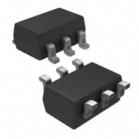
P-TSOP-6-6-3
Type TLE4966H
Package P-TSOP-6-6-3
Functional Description
The TLE4966H is an integrated circuit double Hall-effect sensor designed specifically for highly accurate applications. Precise magnetic switching points and high temperature stability are achieved by active compensation circuits and chopper techniques on chip. The TLE4966H provides a speed signal at Q2 for every magnetic pole pair and a direction information at Q1. The direction output switches 1µs (min.) before the speed output.
�TLE4966H
Circuit Description
The chopped Double Hall Switch comprises two Hall probes, bias generator, compensation circuits, oscillator, and output transistors. The bias generator provides currents for the Hall probes and the active circuits. Compensation circuits stabilize the temperature behavior and reduce technology variations. The Active Error Compensation rejects offsets in signal stages and the influence of mechanical stress to the Hall probes caused by molding and soldering processes and other thermal stresses in the package. This chopper technique together with the threshold generator and the comparator ensures high accurate magnetic switching points.
Figure 1: Block Diagram
Data Sheet
2/11
2003-11-20
�TLE4966H
Pin Configuration
Figure 2: Pin Configuration
Pin Definition and Functions P-TSOP-6-6-3 package
Pin 1 2 3 4 5 6 Symbol Function
Q2 GND Q1 Vs GND GND
Speed Recommended connection to GND Direction Supply voltage Recommended connection to GND Ground
Data Sheet
3/11
2003-11-20
�TLE4966H
Absolute Maximum Ratings
Tj = -40 to 150°C
Parameter Supply Voltage Supply Current through protection device Output Voltage Continuous Output Current Junction Temperature Symbol VS IS VQ IQ Tj min. -18 -18 -18 -50 -0.7 -0,7 -50 max. 18 24 26 +50 18 26 +50 Unit V mA V for 5 min @ 1.2 kOhm pull up mA Conditions for 1h ,Rs>=200 Ohm for 5min, Rs>=200 Ohm
155 °C for 2000 h (not additive) 165 for 1000 h (not additive) 175 for 168 h (not additive) 195 for 3x1 h (additive) Storage Temperature TS -40 150 °C Magnetic Flux Density B unlimit. mT Note: Stresses above those listed here may cause permanent damage to the device. Exposure to absolute maximum rating conditions for extended periods may affect device reliability.
ESD Protection
Human Body Model (HBM) tests according to: EOS/ESD Association Standard S5.1-1993 and Mil. Std. 883D method 3015.7
Parameter ESD Voltage Symbol VESD max. ±4 Unit kV Conditions HBM, R= 1.500 Ohm, C= 100pF; TA = 25°C
Operating Range
Parameter Supply Voltage Output Voltage Junction Temperature Output Current Symbol VS VQ Tj IQ min. 2.7 -0.7 -40 0 typ. max. 18 24 26 18 150 175 10 Unit V V °C for 168 h mA Conditions 1h with RS >= 200 Ohm for 5min RS >=2 00 Ohm
Data Sheet
4/11
2003-11-20
�TLE4966H
AC/DC Characteristics
over operating range, unless otherwise specified. Typical values correspond to VS=12V and TA=25°C.
Parameter Supply Current Reverse Current Output Saturation Voltage Output Leakage Current Output Fall Time Output Rise Time Chopper Frequency Switching Frequency 2) Delay Time Delay of Count Signal 3) Output Jitter Symbol IS ISR VQSAT IQLEAK tf tr fOSC fSW td td,count tQJ min. 3 0 0 typ. 5.5 0.2 0.3 0.05 0.2 0.2 320 13 1 1 max. 8 1 0.6 10 1 1 1) 15 Unit mA mA V µA µs µs Conditions VS = 2.7V .. 18V VS= -18V IQ= 10mA for VQ=18 V RL= 1.2 kOhm ;CL Power Dissipation Pdis= 72.0 mW. In TA = Tj – (RthJA * Pdis) = 175 °C – (100 K/W * 0.072 W) => TA = 167.8 °C
kHz kHz µs µs µsRMS Typ. Value for Square-Wave Signal 1kHz µTRMS Typ. Value for ∆B/∆t>12mT/ms µs VS >= 2.7V mm K/W
Data Sheet
5/11
2003-11-20
�TLE4966H
Magnetic Characteristics
over operating range, unless otherwise specified. Typical values correspond to VS=12V.
Parameter Operate Point TLE4966H Release Point TLE4966H Hysteresis TLE4966H Magnetic Matching TLE4966H Magnetic Offset TLE4966H Symbol BOP Tj [°C] -40 25 150 -40 25 150 -40 25 150 -40 25 150 -40 25 150 min. 5.2 5.0 4.7 -10.3 -10.0 -9.5 10.0 -3.0 -3.0 typ. 7.7 7.5 7.1 -7.7 -7.5 -7.1 15.0 0 0 max. 10.3 10.0 9.5 mT -5.2 -5.0 -4.7 mT 20.0 mT 3.0 mT 3.0 Valid for BOP1-BOP2 and BRP1-BRP2 (BOP+BRP)/2 Unit mT Conditions
BRP
BHYS
Bmatch
BOFF
Temperature TC ppm/°C Compensation of -350 Magnetic Thresholds Positive magnetic fields related with south pole of magnet to the branded side of package. Note: Typical characteristics specify mean values expected over the production spread.
Data Sheet
6/11
2003-11-20
�TLE4966H
Timing diagrams for the speed and direction outputs
A p p lie d m a g n e tic fie ld B OP B RP
VQ 90% 10%
tf td
tr
td
Figure 3: Timing definition of the speed signal
Figure 4: Timing Definition of the Direction Signal
Data Sheet
7/11
2003-11-20
�TLE4966H
Figure 5: Definition of the Direction Signal
Rotation Direction left to right right to left Package Dimensions
State of Direction Output VQ1 low high
2.9 ±0.2 (2.25) (0.35)
B Center of sensitive area 0.16 A B
2.6 MAX. 10 ° MAX.
1.1 MAX. 0.1 MAX. 0.62 ±0.05 sensitive area
+0.2 acc. to DIN 6784 0.35
+0.1 -0.05
0.2
M
B 6x 0.2
0.15
M
0.95 1.9
Figure 6: Package Dimension
+0.1 -0.06
A
Data Sheet
8/11
2003-11-20
10° MAX. 1.6 ±0.1
A
�TLE4966H
Figure 7: Foot print
Figure 8: Distance from Package to Die
Data Sheet
9/11
2003-11-20
�TLE4966H
Figure 9: Marking
Data Sheet
10/11
2003-11-20
�TLE4966H
TLE4966H Revision History: Version 1.0 Previous Version: Page Subjects (major changes since last revision)
2003-11-20
For questions on technology, delivery and prices please contact the Infineon Technologies Offices in Germany or the Infineon Technologies Companies and Representatives worldwide: see our webpage at http://www.infineon.com We Listen to Your Comments
Any information within this document that you feel is wrong, unclear or missing at all? Your feedback will help us to continuously improve the quality of this document. Please send your proposal (including a reference to this document) to:
feedback.sensors@infineon.com
Edition 2001-02-22 Published by Infineon Technologies AG St.-Martin-Strasse 53 D-81541 München © Infineon Technologies AG 2000 All Rights Reserved. Attention please! The information herein is given to describe certain components and shall not be considered as warranted characteristics. Terms of delivery and rights to technical change reserved. We hereby disclaim any and all warranties, including but not limited to warranties of noninfringement, regarding circuits, descriptions and charts stated herein. Infineon Technologies is an approved CECC manufacturer. Information For further information on technology, delivery terms and conditions and prices please contact your nearest Infineon Technologies Office in Germany or our Infineon Technologies Representatives worldwide (see address list). Warnings Due to technical requirements components may contain dangerous substances. For information on the types in question please contact your nearest Infineon Technologies Office. Infineon Technologies Components may only be used in life-support devices or systems with the express written approval of Infineon Technologies, if a failure of such components can reasonably be expected to cause the failure of that life-support device or system, or to affect the safety or effectiveness of that device or system. Life support devices or systems are intended to be implanted in the human body, or to support and/or maintain and sustain and/or protect human life. If they fail, it is reasonable to assume that the health of the user or other persons may be endangered.
Data Sheet
11/11
2003-11-20
�
很抱歉,暂时无法提供与“TLE4966H”相匹配的价格&库存,您可以联系我们找货
免费人工找货