May 2010
TLE5011
GMR Angle Sensor
Final
D ata Sheet
V1.1
Sensors
�Edition 2010-05 Published by Infineon Technologies AG 81726 Munich, Germany © 2010 Infineon Technologies AG All Rights Reserved. Legal Disclaimer The information given in this document shall in no event be regarded as a guarantee of conditions or characteristics. With respect to any examples or hints given herein, any typical values stated herein and/or any information regarding the application of the device, Infineon Technologies hereby disclaims any and all warranties and liabilities of any kind, including without limitation, warranties of non-infringement of intellectual property rights of any third party. Information For further information on technology, delivery terms and conditions and prices, please contact the nearest Infineon Technologies Office (www.infineon.com). Warnings Due to technical requirements, components may contain dangerous substances. For information on the types in question, please contact the nearest Infineon Technologies Office. Infineon Technologies components may be used in life-support devices or systems only with the express written approval of Infineon Technologies, if a failure of such components can reasonably be expected to cause the failure of that life-support device or system or to affect the safety or effectiveness of that device or system. Life support devices or systems are intended to be implanted in the human body or to support and/or maintain and sustain and/or protect human life. If they fail, it is reasonable to assume that the health of the user or other persons may be endangered.
�TLE5011
Revision History: 2010-05, V1.1 Previous Revision: V1.0 Page 26 Subjects (major changes since last revision) Table 14, register 0x0D updated
We Listen to Your Comments Any information within this document that you feel is wrong, unclear or missing at all? Your feedback will help us to continously improve the quality of this document. Please send your proposal (including a reference to this document) to:
sensors@infineon.com
Final Data Sheet
3
V1.1, 2010-05
�TLE5011
Table of Contents
Table of Contents
Table of Contents . . . . . . . . . . . . . . . . . . . . . . . . . . . . . . . . . . . . . . . . . . . . . . . . . . . . . . . . . . . . . . . . 4 1 1.1 1.2 1.3 2 2.1 2.2 2.3 2.4 2.5 2.5.1 2.5.2 2.5.3 2.5.4 2.5.5 2.5.6 3 3.1 3.2 3.3 3.4 3.4.1 3.4.2 3.4.3 Product Description . . . . . . . . . . . . . . . . . . . . . . . . . . . . . . . . . . . . . . . . . . . . . . . . . . . . . . . . . . . . . . Overview . . . . . . . . . . . . . . . . . . . . . . . . . . . . . . . . . . . . . . . . . . . . . . . . . . . . . . . . . . . . . . . . . . . . . . . . Features . . . . . . . . . . . . . . . . . . . . . . . . . . . . . . . . . . . . . . . . . . . . . . . . . . . . . . . . . . . . . . . . . . . . . . . . Application Example . . . . . . . . . . . . . . . . . . . . . . . . . . . . . . . . . . . . . . . . . . . . . . . . . . . . . . . . . . . . . . . 6 6 7 7
Functional Description . . . . . . . . . . . . . . . . . . . . . . . . . . . . . . . . . . . . . . . . . . . . . . . . . . . . . . . . . . . . 8 General . . . . . . . . . . . . . . . . . . . . . . . . . . . . . . . . . . . . . . . . . . . . . . . . . . . . . . . . . . . . . . . . . . . . . . . . . 8 Pin Configuration . . . . . . . . . . . . . . . . . . . . . . . . . . . . . . . . . . . . . . . . . . . . . . . . . . . . . . . . . . . . . . . . . 9 Pin Description . . . . . . . . . . . . . . . . . . . . . . . . . . . . . . . . . . . . . . . . . . . . . . . . . . . . . . . . . . . . . . . . . . . 9 Block Diagram . . . . . . . . . . . . . . . . . . . . . . . . . . . . . . . . . . . . . . . . . . . . . . . . . . . . . . . . . . . . . . . . . . 10 Functional Block Description . . . . . . . . . . . . . . . . . . . . . . . . . . . . . . . . . . . . . . . . . . . . . . . . . . . . . . . 11 Internal Power Supply . . . . . . . . . . . . . . . . . . . . . . . . . . . . . . . . . . . . . . . . . . . . . . . . . . . . . . . . . . . 11 GMR Voltage Regulator VRG (VDDG-Voltage) . . . . . . . . . . . . . . . . . . . . . . . . . . . . . . . . . . . . . . . . 11 Analog Voltage Regulator VRA (VDDA-Voltage) . . . . . . . . . . . . . . . . . . . . . . . . . . . . . . . . . . . . . . . 11 Digital Voltage Regulator VRD (VDDD-Voltage) . . . . . . . . . . . . . . . . . . . . . . . . . . . . . . . . . . . . . . . 11 Phase-Locked Loop (PLL) . . . . . . . . . . . . . . . . . . . . . . . . . . . . . . . . . . . . . . . . . . . . . . . . . . . . . . . . 11 Safety Features . . . . . . . . . . . . . . . . . . . . . . . . . . . . . . . . . . . . . . . . . . . . . . . . . . . . . . . . . . . . . . . . 12 Specification . . . . . . . . . . . . . . . . . . . . . . . . . . . . . . . . . . . . . . . . . . . . . . . . . . . . . . . . . . . . . . . . . . . Application Circuit . . . . . . . . . . . . . . . . . . . . . . . . . . . . . . . . . . . . . . . . . . . . . . . . . . . . . . . . . . . . . . . . Absolute Maximum Ratings . . . . . . . . . . . . . . . . . . . . . . . . . . . . . . . . . . . . . . . . . . . . . . . . . . . . . . . . Operating Range . . . . . . . . . . . . . . . . . . . . . . . . . . . . . . . . . . . . . . . . . . . . . . . . . . . . . . . . . . . . . . . . Characteristics . . . . . . . . . . . . . . . . . . . . . . . . . . . . . . . . . . . . . . . . . . . . . . . . . . . . . . . . . . . . . . . . . . Electrical Parameters . . . . . . . . . . . . . . . . . . . . . . . . . . . . . . . . . . . . . . . . . . . . . . . . . . . . . . . . . . . . ESD Protection . . . . . . . . . . . . . . . . . . . . . . . . . . . . . . . . . . . . . . . . . . . . . . . . . . . . . . . . . . . . . . . . GMR Parameters . . . . . . . . . . . . . . . . . . . . . . . . . . . . . . . . . . . . . . . . . . . . . . . . . . . . . . . . . . . . . . . Offset and Amplitude . . . . . . . . . . . . . . . . . . . . . . . . . . . . . . . . . . . . . . . . . . . . . . . . . . . . . . . . . . Offset Definition . . . . . . . . . . . . . . . . . . . . . . . . . . . . . . . . . . . . . . . . . . . . . . . . . . . . . . . . . . . . . . Amplitude Definition . . . . . . . . . . . . . . . . . . . . . . . . . . . . . . . . . . . . . . . . . . . . . . . . . . . . . . . . . . . Temperature-dependent behavior . . . . . . . . . . . . . . . . . . . . . . . . . . . . . . . . . . . . . . . . . . . . . . . . Orthogonality Definition . . . . . . . . . . . . . . . . . . . . . . . . . . . . . . . . . . . . . . . . . . . . . . . . . . . . . . . . Calibration . . . . . . . . . . . . . . . . . . . . . . . . . . . . . . . . . . . . . . . . . . . . . . . . . . . . . . . . . . . . . . . . . . . . . . GMR Values . . . . . . . . . . . . . . . . . . . . . . . . . . . . . . . . . . . . . . . . . . . . . . . . . . . . . . . . . . . . . . . . Temperature Measurement . . . . . . . . . . . . . . . . . . . . . . . . . . . . . . . . . . . . . . . . . . . . . . . . . . . . . Calibration Conditions . . . . . . . . . . . . . . . . . . . . . . . . . . . . . . . . . . . . . . . . . . . . . . . . . . . . . . . . . Angle Calculation . . . . . . . . . . . . . . . . . . . . . . . . . . . . . . . . . . . . . . . . . . . . . . . . . . . . . . . . . . . . . . . . Components of the Output Signals . . . . . . . . . . . . . . . . . . . . . . . . . . . . . . . . . . . . . . . . . . . . . . . . . GMR Error Compensation . . . . . . . . . . . . . . . . . . . . . . . . . . . . . . . . . . . . . . . . . . . . . . . . . . . . . . . . Temperature-dependent Offset Value . . . . . . . . . . . . . . . . . . . . . . . . . . . . . . . . . . . . . . . . . . . . . Offset Correction . . . . . . . . . . . . . . . . . . . . . . . . . . . . . . . . . . . . . . . . . . . . . . . . . . . . . . . . . . . . . Amplitude Normalization . . . . . . . . . . . . . . . . . . . . . . . . . . . . . . . . . . . . . . . . . . . . . . . . . . . . . . . Non-Orthogonality Correction . . . . . . . . . . . . . . . . . . . . . . . . . . . . . . . . . . . . . . . . . . . . . . . . . . . Resulting Angle . . . . . . . . . . . . . . . . . . . . . . . . . . . . . . . . . . . . . . . . . . . . . . . . . . . . . . . . . . . . . . GMR Parameters after Calibration . . . . . . . . . . . . . . . . . . . . . . . . . . . . . . . . . . . . . . . . . . . . . . . . . Signal Processing . . . . . . . . . . . . . . . . . . . . . . . . . . . . . . . . . . . . . . . . . . . . . . . . . . . . . . . . . . . . . . . . Clock Supply (CLK Timing Definition) . . . . . . . . . . . . . . . . . . . . . . . . . . . . . . . . . . . . . . . . . . . . . . . . . Synchronous Serial Communication Interface (SSC) . . . . . . . . . . . . . . . . . . . . . . . . . . . . . . . . . . . . . SSC Timing Definition . . . . . . . . . . . . . . . . . . . . . . . . . . . . . . . . . . . . . . . . . . . . . . . . . . . . . . . . . . . SSC Timing Diagram . . . . . . . . . . . . . . . . . . . . . . . . . . . . . . . . . . . . . . . . . . . . . . . . . . . . . . . . . . 4 13 13 13 14 15 15 16 16 16 17 17 17 17 18 18 18 18 18 18 18 18 19 19 19 19 20 20 21 21 22 22
3.5
3.6 3.6.1 3.6.2
3.6.3 3.7 3.8 3.9 3.9.1
Final Data Sheet
V1.1, 2010-05
�TLE5011
Table of Contents
3.9.2 3.9.3
3.9.4 3.9.5
3.9.6 3.9.7 3.9.8
3.10 3.10.1 3.10.2 3.10.3 3.11 3.11.1 3.11.2 3.11.3 3.11.4 4 4.1
SSC Baud rate . . . . . . . . . . . . . . . . . . . . . . . . . . . . . . . . . . . . . . . . . . . . . . . . . . . . . . . . . . . . . . . . . SSC Spike Filter . . . . . . . . . . . . . . . . . . . . . . . . . . . . . . . . . . . . . . . . . . . . . . . . . . . . . . . . . . . . . . . SSC Spike Filter Off . . . . . . . . . . . . . . . . . . . . . . . . . . . . . . . . . . . . . . . . . . . . . . . . . . . . . . . . . . . SSC Spike Filter On . . . . . . . . . . . . . . . . . . . . . . . . . . . . . . . . . . . . . . . . . . . . . . . . . . . . . . . . . . . Filter for DATA and CS . . . . . . . . . . . . . . . . . . . . . . . . . . . . . . . . . . . . . . . . . . . . . . . . . . . . . . . . SSC Data Transfer . . . . . . . . . . . . . . . . . . . . . . . . . . . . . . . . . . . . . . . . . . . . . . . . . . . . . . . . . . . . . SSC Command Byte . . . . . . . . . . . . . . . . . . . . . . . . . . . . . . . . . . . . . . . . . . . . . . . . . . . . . . . . . . . . Register Table . . . . . . . . . . . . . . . . . . . . . . . . . . . . . . . . . . . . . . . . . . . . . . . . . . . . . . . . . . . . . . . Bit Types . . . . . . . . . . . . . . . . . . . . . . . . . . . . . . . . . . . . . . . . . . . . . . . . . . . . . . . . . . . . . . . . . . . Reserved Registers (08H to 0BH) . . . . . . . . . . . . . . . . . . . . . . . . . . . . . . . . . . . . . . . . . . . . . . . . . Data Communication via SSC . . . . . . . . . . . . . . . . . . . . . . . . . . . . . . . . . . . . . . . . . . . . . . . . . . . . . CRC Generation . . . . . . . . . . . . . . . . . . . . . . . . . . . . . . . . . . . . . . . . . . . . . . . . . . . . . . . . . . . . . . . Slave-active Byte Generation . . . . . . . . . . . . . . . . . . . . . . . . . . . . . . . . . . . . . . . . . . . . . . . . . . . . . Example1: CRC calculation (Update X and Y and set ADC-Test Mode) . . . . . . . . . . . . . . . . . . . Example2: Use of two TLE5011 units in a bus mode. . . . . . . . . . . . . . . . . . . . . . . . . . . . . . . . . Test Structures . . . . . . . . . . . . . . . . . . . . . . . . . . . . . . . . . . . . . . . . . . . . . . . . . . . . . . . . . . . . . . . . . . Functional Angle Tests . . . . . . . . . . . . . . . . . . . . . . . . . . . . . . . . . . . . . . . . . . . . . . . . . . . . . . . . . . ADC Test Vectors . . . . . . . . . . . . . . . . . . . . . . . . . . . . . . . . . . . . . . . . . . . . . . . . . . . . . . . . . . . . Temperature Measurement . . . . . . . . . . . . . . . . . . . . . . . . . . . . . . . . . . . . . . . . . . . . . . . . . . . . . . . Functional Angle Test and Temperature Measurement Timing . . . . . . . . . . . . . . . . . . . . . . . . . . . . Overvoltage Comparators . . . . . . . . . . . . . . . . . . . . . . . . . . . . . . . . . . . . . . . . . . . . . . . . . . . . . . . . . . Internal Supply Voltage Comparators . . . . . . . . . . . . . . . . . . . . . . . . . . . . . . . . . . . . . . . . . . . . . . . VDD Overvoltage Detection . . . . . . . . . . . . . . . . . . . . . . . . . . . . . . . . . . . . . . . . . . . . . . . . . . . . . . . GND-off Comparator . . . . . . . . . . . . . . . . . . . . . . . . . . . . . . . . . . . . . . . . . . . . . . . . . . . . . . . . . . . . VDD - off Comparator . . . . . . . . . . . . . . . . . . . . . . . . . . . . . . . . . . . . . . . . . . . . . . . . . . . . . . . . . . . . Package Information . . . . . . . . . . . . . . . . . . . . . . . . . . . . . . . . . . . . . . . . . . . . . . . . . . . . . . . . . . . . Package Parameters . . . . . . . . . . . . . . . . . . . . . . . . . . . . . . . . . . . . . . . . . . . . . . . . . . . . . . . . . . . . . Package Outline PG-DSO-8 . . . . . . . . . . . . . . . . . . . . . . . . . . . . . . . . . . . . . . . . . . . . . . . . . . . . Footprint PG-DSO-8 . . . . . . . . . . . . . . . . . . . . . . . . . . . . . . . . . . . . . . . . . . . . . . . . . . . . . . . . . . Packing . . . . . . . . . . . . . . . . . . . . . . . . . . . . . . . . . . . . . . . . . . . . . . . . . . . . . . . . . . . . . . . . . . . . Marking . . . . . . . . . . . . . . . . . . . . . . . . . . . . . . . . . . . . . . . . . . . . . . . . . . . . . . . . . . . . . . . . . . . . Processing . . . . . . . . . . . . . . . . . . . . . . . . . . . . . . . . . . . . . . . . . . . . . . . . . . . . . . . . . . . . . . . . . .
24 24 24 24 25 25 25 26 26 29 32 33 33 34 35 36 36 37 37 38 39 39 39 39 40 41 41 41 42 42 42 42
Final Data Sheet
5
V1.1, 2010-05
�GMR Angle Sensor
TLE5011
1
1.1
Product Description
Overview
The TLE5011 is a 360° angle sensor that detects the orientation of a magnetic field by measuring sine and cosine angle components with monolithic integrated Giant Magneto Resistance (iGMR) elements. Data communications are accomplished with a bi-directional Synchronous Serial Communication (SSC) interface that is SPI compatible. The sine and cosine values can be read out digitally. These signals can be digitally processed to calculate the angle orientation of the magnetic field (magnet). This calculation can be done by using a COordinate Rotation DIgital Computer (CORDIC) algorithm. It is possible to connect more than one TLE5011 to one SSC interface of a microcontroller for redundancy or any other reason. If multiple TLE5011 devices are used, the synchronization of the connected TLE5011 is performed by a broadcast command. Each connected TLE5011 can be addressed by a dedicated Chip Select CS pin.
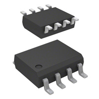
Type TLE5011 Final Data Sheet
Marking 5011
Ordering Code SP000393517 6
Package PG-DSO-8 V1.1, 2010-05
�TLE5011
Product Description
1.2
• • • • • • • • • • • • • • • •
Features
Giant Magneto Resistance (GMR)-based principle Integrated magnetic field sensing for angle measurement Full 0 - 360° angle measurement Highly accurate single-bit SD-ADC 16-bit representation of sine / cosine values on the interface Wide magnetic operating range: 30mT to 50mT Bi-directional SSC interface up to 2 Mbit/s 3-pin SSC interface, SPI compatible with open drain ADCs and filters synchronized with external commands via SSC Test resistors for simulating angle values Core supply voltage 2.5 V 0.25-µm CMOS technology Automotive qualified: -40°C to +150°C (junction temperature) Latch-up immunity according JEDEC standard ESD > 2 kV (HBM) Green package with lead-free (Pb-free) plating
1.3
• • • •
Application Example
The TLE5011 GMR angle sensor is designed for angular position sensing in automotive applications, such as: Steering angle Brushless DC motor commutation (e.g. Electric Power Steering (EPS)) Rotary switch General angular sensing
Final Data Sheet
7
V1.1, 2010-05
�TLE5011
Functional Description
2
2.1
Functional Description
General
The GMR angle sensor is implemented in vertical integration. This means that the GMR active areas are integrated above the logic portion of the TLE5011 device. GMR elements change their resistance depending on the direction of the magnetic field. Four individual GMR elements are connected to one Wheatstone sensor bridge. These GMR elements sense either of two components of the applied magnetic field: • • X component, VX (cosine) Y component, VY (sine)
The advantage of a full-bridge structure is that the amplitude of the GMR signal is doubled.
GMR Resistors
S
0°
VX
VY
N
ADCX+
ADCX -
GND
ADCY +
ADCY-
VDDG
90°
Figure 1 Sensitive Bridges of the GMR Angle Sensor
Note: In Figure 1, the arrows in the resistor symbols denote the direction of the reference layer, which is used for the further explanation (Figure 2). The output signal of each bridge is only unambiguous over 180° between two maxima. Therefore two bridges are orientated orthogonally to each other to measure the 360° angle range. Using the ARCTAN function, the true 360° angle value can be calculated that is represented by the relation of the cosine (here X) and sine (here Y) signals. Because only the relative values influence the result, the absolute size of the two signals is of minor importance. Therefore, most influences on the amplitudes are compensated.
Final Data Sheet
8
V1.1, 2010-05
�TLE5011
Functional Description
Y Component (SIN)
VY VX V
X Component (COS)
VX (COS)
0°
90°
180°
270°
360°
Angle α
VY (SIN)
Figure 2
Ideal Output of the GMR Angle Sensor
2.2
Pin Configuration
8
7
6
5
Center of Sensitive Area
1
Figure 3
2
3
4
Pin Configuration (Top View)
2.3
Table 1
Pin No. 1 2 3 4 5 6 7 8
Pin Description
Pin Describtion
Symbol In/Out Function Chip Clock SSC Clock SSC Chip Select SSC Data, open drain Test Pin 1, must be connected to GND Supply Voltage Ground Test Pin 2, must be connected to GND
CLK SCK CS DATA TST1 VDD GND TST2
I I I I/O I/O I/O
Final Data Sheet
9
V1.1, 2010-05
�TLE5011
Functional Description
2.4
Block Diagram
GND VDD
The block diagram shows all switches in the reset position.
GND-off Comp
TST 1
VDD_max
VDD_OV Comp
VDD-off Comp
CLK SCK SCK
VRG VRG_OV
VRG_Rst
VRA
VRA_OV
VRA_Rst
VRD VRD_OV
VRD_Rst
SSC
DATA CS
GMR X
VDDG
Angle Voltage
Temperature Sensor
A
2 GND VDDG
D
1
Comb Filter
16
FIR Filter 16
XH XL
FSYNC
FCNT
Control FSM
A
2
D
1
Comb 16 Filter
FIR 16 Filter
YH YL
GND
GMR Y
2 differential
Angle Voltage Analog Clock Digital Clock VRG_Rst VRA_Rst VRD_Rst Reset Lock
PLL
CLK
TLE5011
TST1 TST 2
Digital Reset
Figure 4
Block Diagram
Final Data Sheet
10
V1.1, 2010-05
�TLE5011
Functional Description
2.5 2.5.1
• • •
Functional Block Description Internal Power Supply
The internal stages of the TLE5011 are supplied with different voltage regulators: GMR Voltage Regulator VRG Analog Voltage Regulator VRA Digital Voltage Regulator VRD
Each voltage regulator has its own overvoltage and undervoltage detection circuits.
2.5.2
• • •
GMR Voltage Regulator VRG (VDDG-Voltage)
The GMR voltage regulator supplies all GMR parts: GMR bridges Test voltages for angle test ADC reference voltage
The voltages are monitored in the VRG overvoltage and undervoltage detectors.
2.5.3
• • • • •
Analog Voltage Regulator VRA (VDDA-Voltage)
The analog voltage regulator supplies the analog parts: ADCs PLL (analog) VDD-off comparator GND-off comparator VDD Overvoltage detection
The voltages are monitored in the VRA overvoltage and undervoltage detectors.
2.5.4
• • • • •
Digital Voltage Regulator VRD (VDDD-Voltage)
The digital voltage regulator supplies all digital parts: Comb filters, FIR filters PLL (digital) Control FSM with bitmap SSC interface Counters (Reset, FSYNC, FCNT)
The voltages are monitored in the VRD overvoltage and undervoltage detectors.
2.5.5
Phase-Locked Loop (PLL)
The clock for the sensors is provided externally. This ensures synchronous operation in case of multiple system participants. The sensor has its own PLL to generate the necessary clock frequency for the chip operation.
Final Data Sheet
11
V1.1, 2010-05
�TLE5011
Functional Description
2.5.6
Safety Features
The TLE5011 has a multiplicity on safety features to support Safety Integrity Level (SIL). Sensors meeting this performance standard are identified by Infineon with the following logo:
Figure 5
PRO SIL Logo
Safety features are: • • • • • • • • • Angle test (generated via test voltages feeding the ADC). Crossed signal paths (switchable for comparison) Invertable ADC bitstreams Overvoltage and undervoltage detection of internal and external voltages VDD-off and GND-off to detect supply malfunctions Frame counter and synchronisation counter Separate bandgap-reference voltages for regulators and comparators CRC-protected SSC protocol Locked configuration registers
Disclaimer PRO-SIL™ is a Registered Trademark of Infineon Technologies AG The PRO-SIL™ Trademark designates Infineon products which contain SIL Supporting Features. SIL Supporting Features are intended to support the overall System Design to reach the desired SIL (according to IEC61508) or A-SIL (according to ISO26262) level for the Safety System with high efficiency. SIL respectively A-SIL certification for such a System has to be reached on system level by the System Responsible at an accredited Certification Authority. SIL stands for Safety Integrity Level (according to IEC 61508) A-SIL stands for Automotive-Safety Integrity Level (according to ISO 26262)
Final Data Sheet
12
V1.1, 2010-05
�TLE5011
Specification
3
3.1
Specification
Application Circuit
The application circuit shows the microcontroller version with open-drain capabilities.
12V Voltage Regulator
VDD
SSC
CLK DATA_o
each 100 R
1k VDD 100 R
CAN RX CAN TX
CAN Tranceiver
CAN µController Master
DATA_i SCK CSQ
GMR-Sensor TLE5011
GND
100 nF
GND
Figure 6
Application Circuit
A complete system may consist of one TLE5011 and a microcontroller. The second TLE5011 may be used for redundancy to increase system reliability. The microcontroller should contain a CORDIC coprocessor for fast angle calculations, and flash memory for the calibration data storage.
3.2
Table 2 Parameter
Absolute Maximum Ratings
Absolute Maximum Rating Parameters Symbol -0.5 -0.5 -40 Limit Values min. max. 6.5 6.5 150 150 |125| |100| |70| |60| 150 °C V V °C °C mT for 1000 h not additive max 5 min. @ tA = 25°C max 5 h @ tA = 25°C max 1000 h @ tA = 85°C not additive max 1000 h @ tA = 100°C not additive without magnetic field max 40 h / lifetime
VDD + 0.5 V may not be exceeded
Unit
Notes
Voltage on VDD pin with respect VDD to ground (VSS) Voltage on any pin with respect to ground (VSS) Junction temperature Magnetic field induction
VIN TJ
B
Storage temperature
TST
-40
Note: Stresses above the max. values listed here may cause permanent damage to the device. Exposure to absolute maximum rating conditions for extended periods may affect device reliability. Maximum ratings are absolute ratings; exceeding only one of these values may cause irreversible damage to the integrated circuit.
Final Data Sheet
13
V1.1, 2010-05
�TLE5011
Specification
3.3
Operating Range
To ensure correct operation of the TLE5011, the operating conditions identified in Table 3 must not be exceeded. All parameters specified in the following sections refer to these operating conditions, unless otherwise indicated. Table 3 is valid for -40°C < TJ < 150°C Table 3 Parameter Supply Voltage Output Current Input Voltage Magnetic Induction Angle Range
1) 2) 3) 4)
Operating Range Symbol
VDD IQ VIN BXY Ang
Limit Values min. 4.5 -0.3 30 0 typ. -5 max. 5.5 -10 5.5 50 360
Unit V mA V mT °
Notes
1) 2) 3)
VDD + 0.35 V may not be exceeded
In X / Y direction4) sine / cosine
Directly blocked with 100-nF ceramic capacitor Maximum current to GND over Open Drain Output The corresponding voltage levels are listed in Table 4 “Electrical Parameters” on Page 15 Values refer to a homogenous magnetic field (Bxy) without vertical magnetic induction (Bz = 0 mT). Applying vertical magnetic induction may cause an additional error.
Note: The thermal resistances listed in Table 19 “Package Parameters” on Page 41 must be used to calculate the corresponding ambient temperature.
Calculation of the Junction Temperature
The total power dissipation PTOT of the chip increases its temperature above the ambient temperature. The power multiplied by the total thermal resistance RthJA (Junction to Ambient) leads to the final junction temperature. RthJA is the sum of the addition of the values of the two components Junction to Case and Case to Ambient.
RthJA = RthJC + RthCA TJ = TA + ΔT ΔT = RthJA x PTOT = RthJA x ( VDD x IDD + VOUT x IOUT )
Example (assuming no load on Vout): – VDD = 5 V – IDD = 15 mA – ΔT =150 [K/W] x (5 [V] x 0.015 [A] + 0 [VA] ) = 11.25 K
IDD , IOUT > 0, if direction is into IC
For moulded sensors, the calculation with RthJC is more adequate.
Final Data Sheet
14
V1.1, 2010-05
�TLE5011
Specification
3.4 3.4.1
Characteristics Electrical Parameters
The indicated electrical parameters apply to the full operating range, unless otherwise specified. The typical values correspond to a supply voltage VDD = 5.0 V and 25°C, unless individually specified. All other values correspond to - 40°C < TJ < 150°C. Table 4 Parameter Supply Current POR Level POR Hysteresis Power-On Time PLL Jitter ADC Noise 5) Input Signal Low Level Input Signal High Level Capacitance of SSC Data Pin Input Hysteresis Pull-Up Current Pull-Down Current
1)
Electrical Parameters Symbol
IDD VPOR VPORhy tPon tPLLjit_S tPLLjit_L NADC VL VH CLDATA VHY IPU IPD
Limit Values min. 2.0 50 -0.35 0.7 VDD 0.07 VDD -10 15 15 10 typ. 15 2.3 30 100 1.3 3.0 1 2 4 max. 20 21 2.9 200 2.0 2) 3.9 2.2 4.4
2)
Unit mA V mV µs ns digits V V pF V µA µA
Notes
VDD = 4.5 to 5.5V VDD = 6.5 V
Power-On Reset
VDD > VDDmin & after first edge on fCLK
short term 3) long term 4) 1 σ @ FIR_BYP = 0 1 σ @ FIR_BYP = 1 Tested only at DATA pin as structures of all pins are identical Internal
0.3 VDD VDD +0.35 6 2) -150 225 225 150 0.7 0.4
CS, DATA
SCK, CLK TST1 TST2
Output Signal Low Level
1) 2) 3) 4) 5)
VOL
-
V
IQ = - 10 mA IQ = - 5 m A 6 )
Without external pull-up resistor for SSC interface Not tested From pulse to pulse Accumulated over 1 ms ADC noise with respect to the peak ADC value specified in “Signal Processing” on Page 20. Noise tested using 1 σ of 100 sample values from Angle Test “000” 6) The value -5 mA is not tested
Note: Table 4 is valid for 4.5V < VDD < 5.5V.
Final Data Sheet
15
V1.1, 2010-05
�TLE5011
Specification
3.4.2
Table 5 Parameter
ESD Protection
ESD Protection Symbol
VHBM VSDM
Limit Values min. max. ±2 ± 500 -
Unit kV V
Notes HBM 1) SDM 2)
ESD Voltage
1) Human Body Model (HBM) according to JEDEC EIA/JESD22-A114-B (R = 1.5 kΩ, C = 100 pF, TA = 25°C) 2) Socketed Device Model (SDM) according to ESD ASS.STD.DS5.3-93
3.4.3
Table 6 Parameter
GMR Parameters
Basic GMR Parameters Symbol
RGADC AX, AY
2)
All parameters apply over the full operating range, unless otherwise specified. Limit Values min. X, Y Output range X, Y Amplitude
1)
Unit max. ±23230 15781 20620 120 3000 10.0 5000 % digits ° digits digits digits
Notes
typ. 9500 100 0 0 -
6000 3922 80 -3000 -10.0 -5000
at calibration conditions Operating Range at calibration conditions at calibration conditions at calibration conditions without magnet4)
X, Y Synchronism X, Y Offset
3)
k OX, OY
X, Y Orthogonality Error X, Y without field
1) 2) 3) 4)
j
X0, Y 0
See Figure 2 k = 100 x ( AX / AY ). OSIN = ( YMAX + YMIN ) / 2 ; OCOS = ( XMAX + XMIN ) / 2 Not tested
Offset and Amplitude
VY
+A 0° 0 -A 90° 180° 270° 360°
Offset
Angle
Figure 7
Offset and Amplitude Definition
Final Data Sheet
16
V1.1, 2010-05
�TLE5011
Specification Offset Definition The offset of the X and Y signals is defined as the mean value between the signed maximum and minimum values of the idealized sine or cosine wave.
X MAX + X MIN O X = ---------------------------------
2
Y MAX + Y MIN O Y = --------------------------------
2
Amplitude Definition The amplitude is defined as half the difference between the signed maximum and minimum values of the idealized sine or cosine wave.
X MAX – X MIN A X = --------------------------------
2 2
Y MAX – Y MIN A Y = -------------------------------Temperature-dependent behavior The temperature offset gradients for both channels depend on the value at 25°C. The gradients can be calculated using the following linear equations:
KT OX = tco_d_x + ( tco_k_x × O X25 ) KT OY = tco_d_y + ( tco_k_y × O Y25 )
OX25, OY25: Offset values at 25°C in digits.
The application note “TLE5011 Calibration” describes in chapter 2.3, how to determine the coefficients (KTOX, KTOY). Orthogonality Definition The corresponding maximum and zero-crossing points of the SIN and COS signals do not occur at the precise distance of 90°. The difference between X and Y phase is called the orthogonality error.
ϕ = ϕX – ϕY
jideal = 0° jX : Phase error of X (= cos) signal jY : Phase error of Y (= sin) signal
Final Data Sheet
17
V1.1, 2010-05
�TLE5011
Specification
3.5
Calibration
GMR Values The end-of-line calibration can be accomplished using following sequence: 1. 2. 3. 4. 5. 6. Turn magnetic field 360° left and measure X and Y values Calculate amplitude, offset, phase correction values of left turn Turn further 90° left and 90° back right without measurement Turn magnetic field 360° right and measure X and Y values Calculate amplitude, offset, phase correction values of right turn Calculate mean values of amplitude, offset, phase correction values
The conditions are specified in Table 7. The values obtained from this sequence must be stored in a non-volatile memory. They are used for the correction of the read-out X and Y values before the angular calculation. The resulting angular deviation is calculated using the parameters determined above. Temperature Measurement The signal amplitude T25 of the temperature measurement path at the calibration conditions must be measured and stored. Calibration Conditions All errors are related to calibration performed by Infineon under the following conditions: Table 7 Parameter Flux density Temperature GMR test calibration conditions at IFX Symbol
BCAL TCAL
Limit Values min. typ. 30 25 max. -
Unit mT °C
Notes
BZ = 0 m T
3.6 3.6.1
Angle Calculation Components of the Output Signals
The X and Y signals at the output can be described by the following equations:
X = A X × cos ( α + ϕ X ) + O X Y = A Y × sin ( α + ϕ Y ) + O Y
AX : Amplitude of X (= cos) signal OX : Offset of X (= cos) signal AY : Amplitude of Y (= sin) signal OY : Offset of Y (= sin) signal
ϕX : Phase error of X (= cos) signal
ϕY : Phase error of Y (= sin) signal
3.6.2
GMR Error Compensation
Temperature-dependent Offset Value To increase the accuracy, the temperature-dependent offset drift can be compensated. The temperature of the chip must be read out. The offset values OX and OY can be described by the following equations. Final Data Sheet 18 V1.1, 2010-05
�TLE5011
Specification
KT OX O X = O X25 + ------------- × ( T – T 25 ) S
T
KT OY O Y = O Y25 + ------------- × ( T – T 25 ) S
T
OX25 , OY25 : Offset value at 25°C in digits T25 : Temperature value at 25°C in digits T : Temperature value in digits ST : Sensitivity of the temperature measurement path, (see “Temperature Measurement” on Page 37).
Offset Correction After the X and Y values are read out, the temperature-corrected offset value must be subtracted.
X1 = X – OX Y1 = Y – OY
Amplitude Normalization Next, the X and Y values are normalized using the peak values determined in the calibration.
X1 X 2 = -----AX
Y1 Y 2 = -----AY
Non-Orthogonality Correction The influence of the non-orthogonality can be compensated using thefollowing equation, in which only the Y channel must be corrected.
Y 2 – X 2 × sin ( – ϕ ) Y 3 = ------------------------------------------
cos ( – ϕ )
Resulting Angle After correction of all errors, the resulting angle can be calculated using the arctan function1).
Y3 α = arc tan ⎛ ------⎞ – ϕ X ⎝ X 2⎠
1) Microcontroller function “arctan2(Y3,X2)” to resolve 360°
Final Data Sheet
19
V1.1, 2010-05
�TLE5011
Specification
3.6.3
GMR Parameters after Calibration
After calibration under the conditions specified in Table 7 “GMR test calibration conditions at IFX” on Page 18, the sensor has a remaining error as shown in Table 8. The error value refers to BZ = 0 mT and operating conditions given in Table 3 “Operating Range” on Page 14. Table 8 Parameter Overall Angle Error
1) 2) 3) 4) At 25°C, B=30mT Including hysteresis error At 0h At 1000h
GMR Parameter with Temperature-Dependent Offset Compensation Symbol Limit Values min. typ. 0.7 1)
Unit max. 1.6 2.2 ° °
Notes
2) 3) 2) 4)
αerr
-
3.7
Table 9 Parameter
Signal Processing
Signal Processing Symbol
fCut-Off
Limit Values min. typ. 4.9 19.6
1)
Unit max. kHz
Notes FIR_BYP=0 FIR_BYP=1
Internal Cutoff Frequency (-3dB) of sin or cos Value Update Time of sin or cos Value2) Settle Time
3)
-
tupd
-
81.9 20.5 163.8 41.0 -
23230
µs
FIR_BYP=0 FIR_BYP=1 FIR_BYP=0 FIR_BYP=1
tsettle
-
Peak ADC Output value ADCPk
digits
signed 16-bit integer (2s complement) 4) 5) 6)
1) For 4-MhHz input frequency 2) tupd = 8192 / (25 x fCLK) for FIR_BYP = 0 tupd = 8192 / (100 x fCLK) for FIR_BYP = 1 3) tsettle = 2 x tupd , after change of ADC input source 4) Output values are valid up to this limit. Above it, corrupted results may occur due to non-linearity of the ADC. 5) One digit typically represents 5.166 µV 6) Corresponds to max. GMR output value
Final Data Sheet
20
V1.1, 2010-05
�TLE5011
Specification
3.8
• • •
Clock Supply (CLK Timing Definition)
The clock signal input “CLK” must fulfill certain requirements described in this section: The high or low pulse width must not exceed the specified values, because the PLL needs a minimum pulse width and must be spike filtered. The duty-cycle factor should be 0.5 but can deviate from the values limited by tCLKh(f_min) and tCLKl(f_min). The PLL is triggered at the positive edge of the clock. If more than 2 edges are missing, a chip reset is generated automatically.
tCLK tCLKh t CLKl VH VL t
Figure 8
CLK Timing Definition
Table 10 Parameter
CLK Timing Specification Symbol
fCLK
1)
Limit Values min. typ. 4.00 50 100 25 40 max. 4.2 70 20 20 3.8 30 -
Unit MHz % ns ns MHz MHz ns
Notes
Input Frequency CLK Duty Cycle CLK rise time CLK fall time PLL Frequency Digital Clock Digital Clock Periode
CLKDUTY tCLKr tCLKf fPLL fDIG tDIG
from VL to VH from VH to VL
fCLK * 25
( 25 / 4 ) * fCLK 4 / (25 * fCLK)
1) Minimum duty-cycle factor: tCLKh(f_min) / tCLK(f_min) with tCLK(f_min) = 1 / fCLK(f_min) Maximum duty-cycle factor: tCLKh(f_max) / tCLK(f_min)with tCLKh(f_max) = tCLK(f_min) - tCLKl(min)
3.9
Synchronous Serial Communication Interface (SSC)
The 3-pin SSC interface has a bidirectional data line (open drain), a serial clock signal, and Chip Select. The SSC interface is designed to communicate with a microcontroller with bi-directional SSC interface supporting open drain. Other microcontrollers may require an external NPN transistor. This allows communication with SPI-compatible devices.
Final Data Sheet
21
V1.1, 2010-05
�TLE5011
Specification
µC (SSC Master)
Shift Register
DATA *)
typ. 1k Ω *)
TLE 501x (SSC Slave)
DATA
Shift Register
SCK
*) SCK *) CS
Clock Generator
CS *) optional , e.g. 100 Ω
Figure 9
SSC Half-Duplex Configuration - Microcontroller with Open Drain
µC (SSC Master)
Shift Register
typ. 1kΩ MRST MTSR optional *) SCK *) CS *) optional , e.g. 100 Ω SCK CS *) *) DATA
TLE 501x (SSC Slave)
Shift Register
Clock Generator
Figure 10
SSC Half-Duplex Configuration - Microcontroller without Open Drain
3.9.1
SSC Timing Definition
SSC Timing Diagram
tSCKp tCSs CS SCK tSCKh tSCKl
tCSh
tCSoff VH VL VH VL VH VL
DATA tDATr tDATw
Figure 11
SSC Timing Definition
SSC Inactive Time ( CSoff ) The SSC Inactive Time defines the delay before the TLE5011 can be selected again after a transfer. The TLE5011 reacts only to one command after an SSC Inactive Time. Then the SSC interface of the TLE5011 is disabled until the next SSC Inactive Time occurs.
Final Data Sheet
22
V1.1, 2010-05
�TLE5011
Specification DATA Write Time ( tDATW ) During this time, the TLE5011 changes the data line, so the data are invalid. The DATA Write Time values are defined without a pull-up resistor. Pull-up Time Value ( tPU ) The value in Table 11 “SSC Timing Specification” on Page 23 is estimated at 60 ns. Table 11 Parameter SSC Baud Rate CS Setup Time CS Hold Time CSoff SCK High SCK Low DATA Read Time (Data Valid Time) DATA Write Time (Data Valid Time) 2) DATA slope
1) 2) 3) 4)
SSC Timing Specification Symbol
fSSC tCSs tCSh tCSoff tSCKh tSCKl tDATr tDATw tDATs
Note: Timing must be calculated according to Table 10 “CLK Timing Specification” on Page 21 Limit Values min. 3*tDIG+10 5*tDIG+10 10*tDIG 5*tDIG 5*tDIG 6*tDIG-10 5*tDIG-10 6*tDIG+25 typ. 2.0 20 max. 2.11) 7*tDIG+10 7*tDIG+10 7*tDIG+50 + tPU ns 30 3) ns Falling edge 4) Mbit / s ns ns ns ns ns ns SSC_FILT = 0 SSC_FILT = 1 SSC inactive time Unit Notes
fCLK/2, synchronized to fCLK if fCLK = fCLK(max) tPU is the time generated by the pull-up resistor Not tested Internal slope control of falling edge for data bit transition from VH to VL.
tSCKl MIN
SCK
tSCKh
tDATw MIN
SSC_FILT=0
tDATw MAX
Wr
tPU
Earliest sample timepoint
tDATr MIN tDATr MAX
Rd
SCK
tDATw MIN
SSC_FILT=1
tDATw MAX
Wr
t DATr MIN
tPU
Earliest sample timepoint of second sample from 2 of 3 filter
tDATr MAX
Rd
Figure 12
SSC Interface Timing Details - Worst-Case Specified Timing
Note: The read window includes the sampling of the data bit. For SSC_FILT = 1, the 2-of-3 selection is already considered. Only the two last data values need to be equal. For SSC_FILT = 0, only one sample point is selected.
Final Data Sheet
23
V1.1, 2010-05
�TLE5011
Specification The margin time shown in Table 12 is the time between write access to the SSC data line and the earliest possible sample read of the TLE5011 itself for read-back. It is useful to have a maximum distance between the WRITE and subsequent READ. This ensures a reliable readback of the written data for the Slave-Active Byte generation. Table 12 Maximum Pull-up Time Margin with Worst-Case Specified Timing SSC_TIMING don’t care Min. tPU Margin 1) 90 50 Unit ns Comment 0 1 SSC_FILT
1) Calculation: Margin=tSCKl(min)+tDATwMAX-(tPU)-tDATrMIN.For Margin Slave-active Byte: 1111_1110
Final Data Sheet
33
V1.1, 2010-05
�TLE5011
Specification Example1: CRC calculation (Update X and Y and set ADC-Test Mode) Command Data CRC (init all ‘0’)
00000001 00000101 00000000 ----------------------------------xor 11111111 -------=11111110.0 . .A xor 10001110.1 . . --------.. . = 01110000.10 . .B xor 1000111.01 . . -------.-. . = 0110111.110 . .C xor 100011.101 . . ------.--. . = 10100.0110 . .D xor 10001.1101 . . -----.---. . = 00101.101101 . .E xor 100.011101 . . ---.------ . . = 001.11000001. .F xor 1.00011101. . ---.------ . . =.11011100.0 .G xor.10001110.1 . .--------.. = 1010010.10 .H xor 1000111.01 . -------.. = 10101.1100 .I xor 10001.1101 . ----.----. = 100.000100 .J xor 100.011101 . ---.------ . =01100100. Remainder 10011011 inverted Remainder Transmitted Sequence: Command Data CRC 00000001 00000101 10011011
Final Data Sheet
34
V1.1, 2010-05
�TLE5011
Specification Example2: Use of two TLE5011 units in a bus mode. Table 15 1 2 3 4 5 6 7 8 9 10 11 12 13 14 15 16 17 18 19 Update X,Y of two TLE5011 units, and read first TLE5011 Description Command1) Command2) Data Byte 1 to 01H Data Byte 2 to 02H Data Byte 3 to 03H Data Byte 4 to 04H Data Byte 5 to 05H Data Byte 6 to 06H CRC Slave-active Command
3)
SSC Byte no.
Master transmitting 0_0000_000 (update all TLE5011) 1_0001_110 (read first TLE5011) 1_0001_110 (read second TLE5011) -
TLE5011 transmitting XL XH YL YH FCNT_STAT FSYNC_INV calc. CRC value cccc_nnnn XL XH YL YH FCNT_STAT FSYNC_INV calc. CRC value cccc_nnnn
Data Byte 1 to 01H Data Byte 2 to 02H Data Byte 3 to 03H Data Byte 4 to 04H Data Byte 5 to 05H Data Byte 6 to 06H CRC Slave-active
1) Both TLE5011 are selected (CS1=CS2=active) during this command Byte. 2) CS2 of the second TLE5011 slave is deactivated after the second command Byte. 3) CS1 of the first TLE5011 slave is deactivated after the third command Byte.
Final Data Sheet
35
V1.1, 2010-05
�TLE5011
Specification
3.10
• •
Test Structures
Two different test signal structures are implemented in the TLE5011: Functional Angle Test. In this case, well-known signals feed the ADCs. Temperature Measurement. This is useful to read out the chip temperature for compensation purposes.
3.10.1
Functional Angle Tests
It is possible to feed the ADCs with appropriate values to simulate a certain magnet position and other GMR effects. The values are generated with resistors on the chip. The following X / Y ADC values can be programmed: • • • • 4 points, circle amplitude = 70.7% (0°, 90°, 180°, 270°) 8 points, circle amplitude = 100.0% (0°, 45°, 90°, 135°,180°, 225°, 270°, 315°) 8 points, circle amplitude = 122.1% (35.3°, 54.7°, 125.3°, 144.7°, 215.3°, 234.7°, 305.3°, 324.7°) 4 points, circle amplitude = 141.4% (45°, 135°, 225°, 315°)
Note: The 100% values typically correspond to 21700 digits and a voltage of ~ 110 mV.
Table 16
Functional Angle Test X / Y Values (decimal) min. typ. 0 15500 21700 32767 0 -15500 -21700 -32768 max. 400 16200 22700 400 -14800 -20700 -400 14800 20700
Register bits 000 001 010 011 100 101 110 111
1) Not allowed to use.
1)
-400 -16200 -22700
Final Data Sheet
36
V1.1, 2010-05
�TLE5011
Specification ADC Test Vectors
Y
122.1% 141.4%
0% 70.7%
100.0%
X
Figure 16
ADC Test Vectors
3.10.2
Temperature Measurement
An internal bandgap voltage can be used to measure the temperature on the chip. This may be used to compensate for temperature-dependent errors. The temperature values is sent out instead of the X value. Table 17 Parameter Value at -40°C Value at 25°C Value at 150°C Temperature Sensitivity Temperature Measurement Symbol
T-40 T25 T150 ST
Limit Values min. +2550 -22000 typ. +5775 -188.75 max. +22000 +9000 -
Unit digits digits digits dig / K
Notes
1)
1) Should be used for temperature compensation of offset errors
Final Data Sheet
37
V1.1, 2010-05
�TLE5011
Specification
3.10.3
Functional Angle Test and Temperature Measurement Timing
The functional angle test and the temperature readout are based on the same mechanism. In the Normal Mode, the output path is linked to the functional angle test or to the temperature measurement unit until the mode is terminated.
< tupd tupd FSYNC (reset) FCNT[4] ADC&Filter X[16],Y[16] Buffer1 ANGT_EN or TEMP_EN Update GMR_OFF 4 Val_G4 Val_G3 5 Val_G5 0 Val_A0 1 Val_A1 Val_A0 tupd tupd
< tupd tupd tupd tupd
2 Val_A2
0 Val_G0
1 Val_G1 Val_G0
2 Val_G2 Val_G1
Val_G4
Val_A1
useful No GMR signal available
Figure 17
Measurement in Normal Mode
In Automatic Mode, the signal is automatically switched back to GMR measurement after the read-out of one value.
< tupd tupd FSYNC (reset) FCNT[4] ADC&Filter X[16],Y[16] Buffer1 ANGT_EN or TEMP_EN Update GMR_OFF No GMR signal available automatic! 4 Val_G4 Val_G3 5 Val_G5 0 Val_A0 1 Val_A1 Val_A0 tupd tupd tupd Updated FCNT=2 0 Val_G0 Val_A1 1 Val_G1 Val_G0 2 Val_G2 Val_G1 tupd tupd
Val_G4
Figure 18
Measurement in Automatic Mode
Final Data Sheet
38
V1.1, 2010-05
�TLE5011
Specification
3.11
Overvoltage Comparators
Various comparators monitor the voltage in order to ensure error-free operation. The overvoltages must be active for at least tDEL to set the test comparator bits in the SSC interface registers. This works as digital spike suppression. Table 18 Parameter Overvoltage Detection Test Comparators Symbol
VOVG VOVA VOVD VDD Overvoltage VDDOV VGNDoff VVDDoff tDEL
Limit Values min. typ. 2.80 2.80 2.80 6.5 0.54 0.48 10 max. -
Unit V V V V V V µs
Notes
GND - off Voltage
VDD - off Voltage
VGNDoff = VGND - VTST1 VVDDoff = VCLK - VDD or VSCK - VDD
Spike filter Delay
The error condition has to last longer than this value (min. 256 clocks of fDIG)
3.11.1
Internal Supply Voltage Comparators
Every voltage regulator has an overvoltage comparator to detect a malfunction. If the nominal output voltage of 2.5 V is larger than VOVG, VOVA and VOVD, then this overvoltage comparator is activated. It sets the VRx_OV bit.
.
VDDA REF VDD VRG VRA VRD GND
+
GND
10µs Spike Filter
xxx_OV
Figure 19
OV Comparator
3.11.2
VDD Overvoltage Detection
The Overvoltage Detection Comparator monitors the external supply voltage at the VDD pin. It activates the STAT_VR (see Figure 19).
3.11.3
GND-off Comparator
The GND-off Comparator is used to detect a voltage difference between the GND pin and TST1 (which must be soldered to GND in the application). It activates the STAT_VR bit. This circuit can detect a disconnection of the Supply GND Pin.
Final Data Sheet
39
V1.1, 2010-05
�TLE5011
Specification
.
VDD VGNDoff TST1 +dV
VDDA
+
GND
GND
10µs Spike Filter
GND_OFF
Figure 20
GND-off Comparator
3.11.4
VDD - off Comparator
The VDD-off Comparator detects a disconnection of the VDD pin supply voltage. In this case, the TLE5011 is supplied by the SCK, CLK and CS input pins via the ESD structures. It activates the STAT_VR bit. The retriggerable analog monoflop is necessary because of the non-static signal of the CLK and SCK signals. This comparator is also activated if spikes on CLK or SCK achieve the condition: (VCLK - VDD) > VVDDoff or (VSCK - VDD) > VVDDoff
.
VDDA VDD VVDDoff CLK SCK GND -dV
+
GND
1µs Mono Flop
10µs Spike Filter
VDD _OFF
Figure 21
VDD - off Comparator
Final Data Sheet
40
V1.1, 2010-05
�TLE5011
Package Information
4
4.1
Table 19 Parameter
Package Information
Package Parameters
Package Parameters Symbol
RthJA RthJC RthJL
Limit Values min. typ. 150 MSL 3 Cu Sn 100% max. 200 75 85 -
Unit K/W K/W K/W
Notes Junction to air 1) Junction to case Junction to lead 260°C > 7 µm
Thermal Resistance
Soldering Moisture Level Lead frame Plating
1) According to Jedec JESD51-7
Package Outline PG-DSO-8
Figure 22
Package Outline PG-DSO-8
Final Data Sheet
41
V1.1, 2010-05
�TLE5011
Package Information Footprint PG-DSO-8
1.31
0.65 5.69 1.27
Figure 23 Packing
Footprint PG-DSO-8
8
0.3
12 ±0.3
5.2
6.4
1.75 2.1
Figure 24 Marking
Tape and Reel
Position 1st Line 2nd Line
Marking
Description See ordering table on page 6 G .. green, S .. series production, y .. year, ww .. cal.week
5011xx GSyww
Processing Note: For processing recommendations, please refer to Infineon’s Notes on Processing
Final Data Sheet
42
V1.1, 2010-05
�www.infineon.com
Published by Infineon Technologies AG
�