物料型号:
- 型号:TLE 6365 G
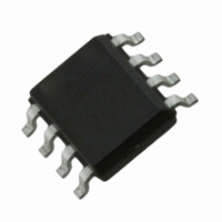
- 封装:PG-DSO-8
- 标记:6365G
器件简介:
- TLE 6365 G是一款专为汽车应用设计的电源电路。
- 基于英飞凌的SPT®技术,集成了双极和CMOS控制电路以及DMOS功率器件。
- 包含降压转换器和上电复位功能,以启动系统。
- 非常小的PG-DSO-8 SMD封装满足应用需求,提供精确的5V输出电压,且具有全面的短路保护功能。
- 内置特性如供电和输出电压的欠压和过压锁定,过温关断功能提高了TLE 6365 G的可靠性。
引脚分配:
- 1号引脚(R):参考输入;通过此引脚和地之间的外部电阻确定参考电流和振荡器/开关频率。
- 2号引脚(RO):复位输出;内部上拉复位比较器的开路输出。
- 3号引脚(BUC):降压转换器补偿输入;内部误差放大器的输出;为环路补偿和稳定性,需连接外部RC串联组合至地。
- 4号引脚(GND):地;模拟信号地。
- 5号引脚(Vcc):输出电压输入;反馈输入(集成电阻分压器)和逻辑供电输入;需要外部阻塞电容器。
- 7号引脚(BUO):降压转换器输出;集成功率DMOS的源极。
- 6号引脚(BDS):降压驱动供电输入;驱动降压转换器功率级所需的电压。
- 8号引脚(Vs):供电电压输入;降压转换器输入电压;需要外部阻塞电容器。
参数特性:
- 工作电压范围宽泛,环境工作温度为-40°C至125°C,供电电压范围宽泛。
- 非常低的电流消耗,符合绿色环保产品标准(RoHS合规)。
- 通过AEC认证。
功能详解:
- TLE 6365 G包含一个降压转换器和一个上电复位功能,用于启动系统。
- 输出电压为5V,具有短路保护功能。
- 内置多种保护功能,如供电和输出电压的欠压和过压锁定,过温关断功能。
应用信息:
- 适用于需要稳定逻辑电源电压(典型值为5V)的系统,通过外部降压电感PWM切换实现。
封装信息:
- PG-DSO-8封装,符合RoHS合规的小外形尺寸。