Data Sheet, Rev. 1.2, Nov. 2007
TLE7269G
Twin LIN Transceiver
Automotive Power
�TLE7269G
Table of Contents
Table of Contents
1 2 3 3.1 3.2 4 4.1 4.2 4.2.1 4.2.2 4.2.3 4.3 4.4 4.5 4.6 4.7 4.8 4.9 4.10 4.11 4.12 4.13 4.14 4.15 5 5.1 5.2 5.3 6 6.1 6.2 7 7.1 7.2 7.3 7.4 7.5 8 9 Overview . . . . . . . . . . . . . . . . . . . . . . . . . . . . . . . . . . . . . . . . . . . . . . . . . . . . . . . . . . . . . . . . . . . . . . . 3 Block Diagram . . . . . . . . . . . . . . . . . . . . . . . . . . . . . . . . . . . . . . . . . . . . . . . . . . . . . . . . . . . . . . . . . . . 4 Pin Configuration . . . . . . . . . . . . . . . . . . . . . . . . . . . . . . . . . . . . . . . . . . . . . . . . . . . . . . . . . . . . . . . . 5 Pin Assignment . . . . . . . . . . . . . . . . . . . . . . . . . . . . . . . . . . . . . . . . . . . . . . . . . . . . . . . . . . . . . . . . . . . 5 Pin Definitions and Functions . . . . . . . . . . . . . . . . . . . . . . . . . . . . . . . . . . . . . . . . . . . . . . . . . . . . . . . . 5 Functional Description . . . . . . . . . . . . . . . . . . . . . . . . . . . . . . . . . . . . . . . . . . . . . . . . . . . . . . . . . . . . 7 Operating Modes . . . . . . . . . . . . . . . . . . . . . . . . . . . . . . . . . . . . . . . . . . . . . . . . . . . . . . . . . . . . . . . . . 8 Normal Operation Mode . . . . . . . . . . . . . . . . . . . . . . . . . . . . . . . . . . . . . . . . . . . . . . . . . . . . . . . . . . . . 9 Normal Slope Mode . . . . . . . . . . . . . . . . . . . . . . . . . . . . . . . . . . . . . . . . . . . . . . . . . . . . . . . . . . . . . 10 Low Slope Mode . . . . . . . . . . . . . . . . . . . . . . . . . . . . . . . . . . . . . . . . . . . . . . . . . . . . . . . . . . . . . . . 10 Flash Mode . . . . . . . . . . . . . . . . . . . . . . . . . . . . . . . . . . . . . . . . . . . . . . . . . . . . . . . . . . . . . . . . . . . 11 Stand-By Mode . . . . . . . . . . . . . . . . . . . . . . . . . . . . . . . . . . . . . . . . . . . . . . . . . . . . . . . . . . . . . . . . . . 12 Sleep Mode . . . . . . . . . . . . . . . . . . . . . . . . . . . . . . . . . . . . . . . . . . . . . . . . . . . . . . . . . . . . . . . . . . . . . 13 Wake-Up Events . . . . . . . . . . . . . . . . . . . . . . . . . . . . . . . . . . . . . . . . . . . . . . . . . . . . . . . . . . . . . . . . . 13 Wake-Up Bus2 Off . . . . . . . . . . . . . . . . . . . . . . . . . . . . . . . . . . . . . . . . . . . . . . . . . . . . . . . . . . . . . . . 13 Bus Wake-Up via LIN bus 1 and bus 2 . . . . . . . . . . . . . . . . . . . . . . . . . . . . . . . . . . . . . . . . . . . . . . . . 14 Local Wake-Up . . . . . . . . . . . . . . . . . . . . . . . . . . . . . . . . . . . . . . . . . . . . . . . . . . . . . . . . . . . . . . . . . . 15 Mode Transition via EN pin . . . . . . . . . . . . . . . . . . . . . . . . . . . . . . . . . . . . . . . . . . . . . . . . . . . . . . . . . 15 Power-On Reset . . . . . . . . . . . . . . . . . . . . . . . . . . . . . . . . . . . . . . . . . . . . . . . . . . . . . . . . . . . . . . . . . 16 TxD Time Out function . . . . . . . . . . . . . . . . . . . . . . . . . . . . . . . . . . . . . . . . . . . . . . . . . . . . . . . . . . . . 17 Over Temperature protection . . . . . . . . . . . . . . . . . . . . . . . . . . . . . . . . . . . . . . . . . . . . . . . . . . . . . . . 18 3.3 V and 5 V Logic Capability . . . . . . . . . . . . . . . . . . . . . . . . . . . . . . . . . . . . . . . . . . . . . . . . . . . . . . 18 BUS Short to GND Feature . . . . . . . . . . . . . . . . . . . . . . . . . . . . . . . . . . . . . . . . . . . . . . . . . . . . . . . . 18 LIN Specifications 1.2, 1.3, 2.0 and 2.1 . . . . . . . . . . . . . . . . . . . . . . . . . . . . . . . . . . . . . . . . . . . . . . . 18 General Product Characteristics . . . . . . . . . . . . . . . . . . . . . . . . . . . . . . . . . . . . . . . . . . . . . . . . . . . Absolute Maximum Ratings . . . . . . . . . . . . . . . . . . . . . . . . . . . . . . . . . . . . . . . . . . . . . . . . . . . . . . . . Functional Range . . . . . . . . . . . . . . . . . . . . . . . . . . . . . . . . . . . . . . . . . . . . . . . . . . . . . . . . . . . . . . . . Thermal Characteristics . . . . . . . . . . . . . . . . . . . . . . . . . . . . . . . . . . . . . . . . . . . . . . . . . . . . . . . . . . . 19 19 20 20
Electrical Characteristics . . . . . . . . . . . . . . . . . . . . . . . . . . . . . . . . . . . . . . . . . . . . . . . . . . . . . . . . . 21 Functional Device Characteristics . . . . . . . . . . . . . . . . . . . . . . . . . . . . . . . . . . . . . . . . . . . . . . . . . . . 21 Diagrams . . . . . . . . . . . . . . . . . . . . . . . . . . . . . . . . . . . . . . . . . . . . . . . . . . . . . . . . . . . . . . . . . . . . . . 26 Application Information . . . . . . . . . . . . . . . . . . . . . . . . . . . . . . . . . . . . . . . . . . . . . . . . . . . . . . . . . . ESD Robustness according to IEC61000-4-2 . . . . . . . . . . . . . . . . . . . . . . . . . . . . . . . . . . . . . . . . . . Pin Compatibility to the Single LIN Transceivers . . . . . . . . . . . . . . . . . . . . . . . . . . . . . . . . . . . . . . . . Master Termination . . . . . . . . . . . . . . . . . . . . . . . . . . . . . . . . . . . . . . . . . . . . . . . . . . . . . . . . . . . . . . . External Capacitors . . . . . . . . . . . . . . . . . . . . . . . . . . . . . . . . . . . . . . . . . . . . . . . . . . . . . . . . . . . . . . Application Example . . . . . . . . . . . . . . . . . . . . . . . . . . . . . . . . . . . . . . . . . . . . . . . . . . . . . . . . . . . . . . 28 28 28 29 29 30
Package Outlines . . . . . . . . . . . . . . . . . . . . . . . . . . . . . . . . . . . . . . . . . . . . . . . . . . . . . . . . . . . . . . . 32 Revision History . . . . . . . . . . . . . . . . . . . . . . . . . . . . . . . . . . . . . . . . . . . . . . . . . . . . . . . . . . . . . . . . 34
Data Sheet
2
Rev. 1.2, 2007-11-13
�Twin LIN Transceiver
TLE7269G
1
Features • • • • • • • • • • • • • • • •
Overview
Two stand-alone LIN transceivers up to 20 kBaud transmission rate Pin compatible to single LIN Transceivers (e.g TLE7259-2GE/GU) Compliant to LIN specification 1.3, 2.0, 2.1 and SAE J2602 Very high ESD robustness, ± 8 kV according to IEC61000-4-2 Optimized for low electromagnetic emission (EME) Optimized for high immunity against electromagnetic interference (EMI) Very low current consumption in sleep mode with Wake-Up functions Wake-Up source detection on Wake-Up disable function Very low leakage current on the BUS output Control output for voltage regulator Digital I/O levels compatible for 3.3 V and 5 V microcontrollers Bus short to VBAT protection and Bus short to GND handling Over-temperature and Under-voltage protection Flash mode and Low-Slope Mode Green Product (RoHs compliant) AEC compliant
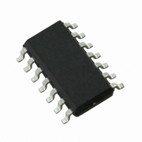
PG-DSO-14
Description The TLE7269G is a transceiver for the Local Interconnect Network (LIN) with integrated Wake-Up and protection features. It is designed for in-vehicle networks using data transmission rates from 2.4 kBaud to 20 kBaud. The TLE7269G functions as a bus driver between the protocol controller and the physical bus inside the LIN network. Compliant to all LIN standards and with a wide operational supply range the TLE7269G can be used in all automotive applications. Two stand-alone LIN transceivers are integrated on one monolithic circuit inside TLE7269G. Both transceivers offer different operation modes and separate INH outputs to control external circuitry, like voltage regulators. In Sleep-mode the TLE7269G draws less than 10 µA of quiescent current for both integrated LIN Transceivers, while both transceivers are still able to wake up off of LIN bus traffic or the local Wake-Up input. The very low leakage current on the BUS pins makes the TLE7269G especially suitable for partially supplied networks and supports the low quiescent current requirements of the LIN network. Based on the Infineon Smart Power Technology SPT®, the TLE7269G provides excellent ESD robustness together with a very high electromagnetic immunity (EMI). The TLE7269G reaches a very low level of electromagnetic emission (EME) within a broad frequency range and independent from the battery voltage. The Infineon Smart Power Technology SPT® allows bipolar and CMOS control circuitry in accordance with DMOS power devices to exist on the same monolithic circuit. The TLE7269G and the Infineon SPT® technology are AEC qualified and tailored to withstand the harsh conditions of the Automotive Environment. Type TLE7269G Data Sheet Package PG-DSO-14 3 Marking 7269G Rev. 1.2, 2007-11-13
�TLE7269G
Block Diagram
2
VS
Block Diagram
14 INH1 13 8 INH2
RBUS
Output Stage 1
Driver
TxD Input
Bus1 12
VS
Current Limit
Timeout
4
TxD1
RTD
Receiver Filter
6
VIO
1
RxD1
Temp Sensor
Wake and Bus Comparators
Mode Control
REN
2
EN
WK
Filter
3
VS RW2O
9
W2O
Receiver Filter
VIO
7 RxD2 10 Bus2
RBUS Output Stage 2
Driver
TxD Input
5
RTD
TxD2
Current Limit
Timeout
11
VS
GND
Figure 1 Data Sheet
Functional Block Diagram 4 Rev. 1.2, 2007-11-13
�TLE7269G
Pin Configuration
3
3.1
Pin Configuration
Pin Assignment
RxD1 EN WK TxD1 TxD2 V IO RxD2
1 2 3 4 5 6 7
14 13 12 11 10 9 8
INH1 VS BUS1 GND BUS2 W2O INH2
Figure 2
Pin Configuration (top view)
Note: The pin configuration of the TLE7269G is pin compatible to the devices TLE7259G and TLE7259-2GE/GU. In comparison to the TLE7259G and the TLE 7259-2GE/GU, no pull up resistors on the RxD pins are required for the TLE7269G. Details can be found inside the “Pin Compatibility to the Single LIN Transceivers” on Page 28.
3.2
Table 1 Pin No. 1 2 3 4 5 6 7
Pin Definitions and Functions
Pin Definitions and Functions Symbol RxD1 EN WK TxD1 TxD2 VIO RxD2 Function Receive data output 1; LOW in dominant state, active LOW after a Wake-Up event at BUS1 or WK pin Enable input; integrated pull-down, device set to normal operation mode when HIGH Wake input; active LOW, negative edge triggered, internal pull-up Transmit data input 1; integrated pull-down, LOW in dominant state; active LOW after Wake-Up via WK pin Transmit data input 2; integrated pull-down, LOW in dominant state Logic Voltage supply input; 3.3V or 5V supply for the RxD and TxD pins Receive data output 2; LOW in dominant state, active LOW after a Wake-Up event at BUS2 5 Rev. 1.2, 2007-11-13
Data Sheet
�TLE7269G
Pin Configuration Table 1 Pin No. 8 Pin Definitions and Functions (cont’d) Symbol INH2 Function Inhibit output 2; battery supply related output HIGH (VS) in Normal and Stand-By operation mode can be used to control an external voltage regulator can be used to control external bus termination resistor when the device will be used as Master node Wake BUS 2 OFF; switch off Wake-Up feature on BUS 2; active HIGH, integrated pull-down Bus 2 input / output; LIN bus line input/output LOW in dominant state Internal termination and pull-up current source Ground Bus 1 input / output; LIN bus line input/output LOW in dominant state Internal termination and pull-up current source Battery supply input Inhibit output 1; battery supply related output HIGH (VS) in Normal and Stand-By operation mode can be used to control an external voltage regulator can be used to control external bus termination resistor when the device will be used as Master node
9
W2O
10
BUS 2
11 12
GND BUS 1
13 14
VS INH1
Data Sheet
6
Rev. 1.2, 2007-11-13
�TLE7269G
Functional Description
4
Functional Description
The LIN Bus is a single wire, bi-directional bus, used for in-vehicle networks. The LIN Transceiver TLE7269G is the interface between the microcontroller and the physical LIN Bus (see Figure 17 and Figure 18). The logical values of the microcontroller are driven to the LIN bus via the TxD inputs of the TLE7269G. The transmit data stream on the TxD input is converted to a LIN bus signal with optimized slew rate to minimize the EME level of the LIN network. The RxD outputs read back the information from the LIN bus to the microcontroller. The receiver has an integrated filter network to suppress noise on the LIN Bus and to increase the EMI (Electro Magnetic Immunity) level of the transceiver. Two logical states are possible on the LIN bus according to the LIN Specification 2.1 (see Figure 3): In dominant state, the voltage on the LIN bus is set to the GND level. In recessive state, the voltage on the LIN bus is set to the supply voltage VS. By setting the TxD1, TxD2 inputs of the TLE7269G to “Low” the transceiver generates a dominant level on the BUS1, BUS2 LIN interface pins. The RxD1, RxD2 outputs read back the signal on the LIN bus and indicate a dominant signal on the LIN bus with a logical “Low” to the microcontroller. Setting the TXD1, TxD2 pins to “High” the transceiver TLE7269G sets the BUS1, BUS2 LIN interface pins to recessive level, at the same time the recessive level on the LIN bus is indicated by a logical “High” on the RxD1, RxD2 outputs. Every LIN network consists of a master node and one or more slave nodes. To configure the TLE7269G for master node applications, a resistor in the range of 1 kΩ and a reverse diode must be connected between the LIN bus and the power supply VS or between the LIN bus and INH pin of the TLE7269G (see Figure 17 and Figure 18). Both integrated transceivers can operate independent from each other and several operation modes and WakeUp functions are implemented. The bus Wake-Up function of the transceiver 2 can be turned off via the W2O pin.
Recessive Dominant Recessive
VIO
TxD1 TxD2
t
VS
Recessive
Dominant
Recessive
BUS1 BUS2
t
VIO
RxD1 RxD2 Recessive Dominant Recessive
Figure 3
LIN bus signals
t
Data Sheet
7
Rev. 1.2, 2007-11-13
�TLE7269G
Functional Description
4.1
Operating Modes
Start-Up Power-Up
Strong Pull Down > 1.5 mA after Wake-Up via pin WK Weak Pull Down 350 kΩ after Power-Up and Wake-Up via BUS1 or BUS2
Note 1:
TxD1: TxD1:
Note 2:
RxD1: RxD1: logical „High“ after Power-Up logical „Low“ after Wake-Up via BUS1 or BUS2 or after Wake-Up via pin WK logical „Low“ after Wake-Up via BUS2
Stand-By Mode
INH1, INH2 = HIGH TxD1 (see Note 1) RxD1, RxD2 (see Note 2)
RxD2:
EN
Go To Normal Operation Mode
EN
LOW HIGH
Status TxD1?
TxD1 EN High Normal Operation Mode
Low Slope Mode
(Transceiver 1 & Transceiver 2) INH1 = HIGH INH2 = HIGH EN = HIGH EN TxD1
TxD1 EN High
Flash Mode
(Transceiver 1 & Transceiver 2) INH1 = High INH2 = High EN = High
Normal Slope Mode
EN TxD1 (Transceiver 1 & Transceiver 2) INH1 = HIGH INH2 = HIGH EN = HIGH
EN
EN
Go To Sleep Mode
EN
LOW
Status W2O ?
HIGH
EN Low
Sleep Mode
INH1/INH2 = Float EN = LOW RxD1/RxD2 = Float
EN Low
Sleep Mode
INH1/INH2 = Float EN = LOW RxD1/RxD2 = Float
Bus Wake-Up feature on BUS2 turned off!
EN
EN
Wake-Up
via via on pin Wk on pin BUS1 or BUS2
Wake-Up
via via on pin Wk on pin BUS1 only !
Figure 4 Data Sheet
Operation Mode State Diagram 8 Rev. 1.2, 2007-11-13
�TLE7269G
Functional Description The TLE7269G has 3 major operation modes: • • • Stand-By mode Normal Operation mode Sleep mode
The Normal Operation mode contains 3 sub-operation modes, which differentiate by the slew rate control of the LIN Bus signal (see Figure 4). Sub-operation modes with different slew rates on the BUS1,BUS2 pins: • • • Low Slope mode, for data transmission rates up to 10.4 kBaud Normal Slope mode, for data transmission rates up to 20 kBaud Flash mode, for programming of the external microcontroller
The TLE7269G contains 2 separate LIN transceivers, which are able to operate in two independent LIN networks with two different data transmission rates. The operation mode of the TLE7269G is selected by the EN pin and the TxD1 pin. Selecting the operation mode applies to the whole device. Transceiver1 and transceiver2 are always set to the same operation mode and sub-operation mode (see Figure 4). Table 2 Mode Sleep Stand-By Operating modes EN Low Low INH1 INH2 TxD1 TXD2 RxD1 RxD2 LIN Bus Comments Termination No Wake-Up request detected RxD1 “Low” after local or bus Wake-Up (BUS 1, BUS 2) RxD2 “Low” after bus Wake-Up on Bus2. RxD2 “High” on all other Wake-Up and Power-Up events. RxD1 “High” after Power-Up TxD1 strong pull down after local Wake-Up (WK pin)2) TxD1 weak pull down after bus Wake-Up (BUS1, BUS2) or Power-Up2) RxD1, RxD2 reflects the signal on the BUS1, BUS2 TxD1,TxD2 driven by the microcontroller
Floating Low High Low High2)
High High resistive Impedance Low High 1) 30 kΩ (typical)
Normal High Operation
High
Low High
Low High
30 kΩ (typical)
1) To indicate the Wake-Up sources via the RxD pins the power supply VIO has to be present 2) The TxD1 input needs an external termination to indicate a “High” or a “Low” signal. The external termination could be a pull-up resistor or an active microcontroller output.
4.2
Normal Operation Mode
The TLE7269G enters the Normal Operation mode after the microcontroller sets EN to “High” (see Figure 4). In Normal Operation mode both LIN bus receivers and both LIN bus transmitters are active. Data from the microcontroller is transmitted to the LIN bus1 or LIN bus2 via the TxD1 or TxD2 pin, the receiver detects the data stream on the LIN bus1 or bus2 and forwards it to the RxD1 or RxD2 output pins. In Normal Operation mode, the INH1 pin and the INH2 are “High” (set to VS) and the bus termination is set to 30 kΩ for both integrated transceivers. Normal Slope mode, Low Slope mode and the Flash mode are Normal Operation modes and in these sub-modes the behavior of the INH pin and the bus termination is the same. To set the device into one of these 3 sub-modes the TxD1 pin and the EN pin are used for the sub-operation mode selection. In order to avoid any bus disturbance during a mode change, the output stages of the TLE7269G are disabled and set to recessive state during the mode change procedure. To release the TLE7269G for data communication on the LIN bus1 and LIN bus2, the TxD1 and TxD2 pins need to be set to “High” for the time tto,rec. Data Sheet 9 Rev. 1.2, 2007-11-13
�TLE7269G
Functional Description
4.2.1
Normal Slope Mode
In Normal Slope mode data transmission rates up to 20 kBauds are possible. Setting the EN pin to “High” starts the transition to Normal Operation mode. Depending on the signal on the TxD1 pin, the TLE7269G changes either into Normal Slope mode or Low Slope mode (see Figure 5). The mode change to Normal Slope mode is defined by the time tMODE and the time tTXD,SET. The time tMODE specifies the delay time between the threshold, where the EN pin detects a “High” input signal, and the actual mode change of TLE7269G into Normal Slope mode. The time tTXD,SET defines the setup time in which the TxD1 pin has be set to “High”. After the time tTXD,SET expires, the logical “High” signal on the TxD1 pin has to be stable to put the part into Normal Slope mode. In the time window tMODE - tTXD,SET the TLE7269G makes the transition to Normal Slope mode but remains in StandBy mode until the time tMODE expires. Finally to release the data communication it is required to set the TxD1 and the TxD2 pin to “High” for the time tto,rec.
VEN,ON EN
Mode Transition TxD1 tTxD,SET
Data transmission tto,rec
tMODE
Stand-By Mode / Sleep Mode
Normal Slope Mode
Figure 5
Timing to enter Normal Slope Mode
4.2.2
Low Slope Mode
In Low Slope mode data transmission rates up to 10.4 kBauds are possible. Setting the EN pin to “High” starts the transition to Normal Operation mode. Depending on the signal of the TxD1 pin the TLE7269G changes either into Normal Slope mode or Low Slope mode (see Figure 6). The mode change to Low Slope mode is defined by the time tMODE and the time tTXD,SET. The time tMODE specifies the delay time between the threshold, where the EN pin detects a “High” input signal, and the actual mode change of TLE7269G to Low Slope mode. The time tTXD,SET defines the setup time in which the TxD1 pin can be set to “Low”. After the time tTXD,SET expires, the logical “Low” signal on the TxD1 pin has to be stable to put the part into Low Slope mode. In the time window tMODE - tTXD,SET the TLE7269G makes the transition into Low Slope mode but remains in StandBy mode until the time tMODE expires. Finally to release the data communication it is required to set the TxD1 and the TxD2 pin to “High” for the time tto,rec.
Data Sheet
10
Rev. 1.2, 2007-11-13
�TLE7269G
Functional Description
.
VEN,ON EN
Data transmission TxD1 Mode Transition tMODE
tTxD,SET
tto,rec
Stand-By Mode / Sleep Mode
Low Slope Mode
Figure 6
Timing to enter Low Slope Mode
4.2.3
Flash Mode
In Flash mode it is possible to transmit and receive LIN messages on the LIN bus. The slew rate control mechanism of the LIN bus signal is disabled. This allows higher data transmission rates, disregarding the EMC limitations of the LIN network. The Flash mode is intended to be used during the ECU production for programming the microcontroller via the LIN bus interface. The TLE7269G can be set to Flash mode either from Normal Slope mode or from Low Slope mode (see Figure 4). Flash mode is entered by setting the EN pin to “Low” for the time tfl1 and generating a falling and a rising edge at the TxD1 pin with the timing tfl2, tfl3 and tfl4 (see Figure 7). Leaving the Flash mode by the same sequence, sets the TLE7269G back to its previous state, be that either Normal Slope mode or Low Slope mode. Finally to release the data transmission it is required to set the TxD1 pin and the TxD2 pin to “High” for the time tto,rec. The TLE7269G can be set from Flash mode directly to Sleep mode by switching the EN pin to “Low”. Setting the pin EN to “High” again, the device will return to Flash mode.
Normal Slope Mode Low Slope Mode
Flash Mode
Normal Slope Mode Low Slope Mode
EN
tfl1
tfl1
TxD1 tfl2
Figure 7
Data transmission
Data transm.
tfl3
tfl4
ttorec
tfl2
tfl3
tfl4
ttorec
Timing to enter and exit Flash Mode
Data Sheet
11
Rev. 1.2, 2007-11-13
�TLE7269G
Functional Description
4.3
• • • • •
Stand-By Mode
The Stand-By mode is entered automatically after: A Power-Up event on the supply VS. A bus Wake-Up event on pin BUS1 or pin BUS2. A local Wake-Up event on the pin WK. A power on reset caused by power supply VS or by the power supply VIO In Stand-By mode the Wake-Up sources are monitored by the TxD1, RxD1 and RxD2 pins.
In Stand-By mode no communication on the LIN Bus is possible. The output stages are disabled and the LIN Bus termination remains activated on both integrated transceivers. Only the RxD1, RxD2 and the TxD1 pin are used to indicate the Wake-Up source. The TxD2 pin remains inactive. The RxD1 pin remains “Low” after a local WakeUp event on the pin WK and a bus Wake-Up event on either the bus 1 or the bus 2. The RxD2 pin remains “Low” only after a bus Wake-Up event on the bus 2. A Power-Up event is indicated by a logical “High” on the RxD1 pin. The signal on the TxD1 pin indicates the Wake-Up source, a weak pull-down signals a bus Wake-Up event on the bus 1 and bus 2 and a strong pull-down signals a local Wake-Up event caused by the WK pin (see Table 2 and Table 3). In order to detect a Wake-Up event via the TxD1 pin, the external microcontroller output needs to provide a logical “High” signal. The Wake-Up flags indicating the Wake-Up source on the pins TxD1, RxD1 and RxD2 are reset by changing the operation mode to Normal Operation mode. The signal on the EN pin remains “Low” due to an internal pull-down resistor. Setting the EN pin to “High”, by the microcontroller returns the TLE7269G to Normal Operation mode. In Stand-By mode the INH1 and INH2 outputs are switching to VS. The INH outputs can be used to control external device like a voltage regulator. Table 3 power up Yes No No No Logic table for wake up monitoring
Inputs
WK 1 BUS1 1 BUS2 1 1 1 WakeUp4) RxD1 1 0 0 0
1)
Outputs
RxD2 1 1 1 0
1)
TxD1 1 0 1 1
2)
Remarks No Wake-Up, Power-Up event Wake via wake pin Wake via BUS1 Wake via BUS2
Wake- 1 Up3) 1 1 WakeUp4) 1
1) To indicate the Wake-Up or Power-Up event on the RxD pin, the supply VIO has to be present 2) The TxD1 input needs an external termination to indicate a “High” or a “Low” signal. The external termination could be a pull-up resistor or an active microcontroller output. 3) A local Wake-Up event is considered after a low signal on the pin WK (see Chapter 4.8). 4) A bus Wake-Up event is considered after the low to high transition on the bus (see Chapter 4.7).
Note: In the case of a sequence of Wake-Up events only the first Wake-Up event will be monitored on TxD1, RxD1 and RxD2. Subsequent Wake-Up events are ignored.
Data Sheet
12
Rev. 1.2, 2007-11-13
�TLE7269G
Functional Description
4.4
Sleep Mode
In order to reduce the current consumption the TLE7269G offers a Sleep mode. In Sleep mode the quiescent current on VS and the leakage current on the pins BUS1 and BUS2 are cut back to a minimum. To switch the TLE7269G from Normal Operation mode to Sleep mode, the EN pin has to be set to “Low”. Conversely a logical “High” on the EN pin sets the device directly back to Normal Operation mode (see Figure 4). While the TLE7269G is in Sleep mode the following functions are available: • The output stages are disabled and the internal bus terminations are switched off (High Impedance on the pins BUS1 and BUS2). Internal current sources on the bus pins ensure that the levels on the pins BUS1 and BUS2 remain recessive and protect the LIN network against accidental bus Wake-Up events. The receiver stages are turned off. RxD1, RxD2 output pins are inactive and “High resistive”. The TxD1, TxD2 pins are disabled. The logical state on the TxD1 pin and the TxD2 pin is “Low” due to the internal pull-down resistors. The INH1 and INH2 outputs are switched off and floating. The bus Wake-Up comparator is active and turns the TLE7269G to Stand-By mode in case of a bus Wake-Up event. The WK pin is active and turns the TLE7269G to Stand-By mode in case of a local Wake-Up. The EN pin remains active, switching the EN pin to “High” changes the operation mode to Normal Operation mode.
• • • • • •
4.5
Wake-Up Events
A Wake-Up event changes the operation mode of the TLE7269G from Sleep mode to Stand-By mode. Both integrated transceivers are changing the mode. There are 4 different ways to Wake-Up the TLE7269G from Sleep mode. • • • • Bus or also called remote Wake-Up via a dominant signal on the pin BUS1. Bus or also called remote Wake-Up via a dominant signal on the pin BUS2. Local Wake-Up via a minimum dominant time (tWK) on the WK pin. Mode change from Sleep mode to Normal Operation mode, by setting EN pin to logical “High”.
4.6
Wake-Up Bus2 Off
A Wake-Up event on the LIN bus1 or on the bus2 wakes up the TLE7269G and sets it to Stand-By mode. In applications where a Wake-Up via bus1 is required but a Wake-Up via bus2 is not wanted, the bus Wake-Up event on the BUS2 can be disabled. This is done by setting the W2O pin to “High”. During the mode change from Normal Operation mode to Sleep mode the TLE7269G checks for the status on the pin W2O. In case the W2O pin is “High”, the Wake-Up feature for the transceiver 2 will be disabled. The TLE7269G can still be wake off by a bus Wake-Up event on LIN bus1 or by a local Wake-Up event on the pin WK. A bus Wake-Up event on the bus 2 won’t be recognized and the device remains in Sleep mode (see Figure 4). In case the Wake-Up Bus2 Off feature is not used, the W2O pin can be left open, due to the internal pull-down resistor, a not connected W2O pin is set to logical “Low”. The function of the EN pin remain unchanged.
Data Sheet
13
Rev. 1.2, 2007-11-13
�TLE7269G
Functional Description
4.7
Bus Wake-Up via LIN bus 1 and bus 2
LIN BUS1 or BUS2 Signal VBUS1 &2
VBUS,wk VBUS,dom tWK,bus
Sleep Mode
Stand-By Mode
INH1/ INH2
Figure 8
Bus Wake-Up behavior
The bus Wake-Up event, often called remote Wake-Up, changes the operation mode from Sleep mode to StandBy mode. The TLE7269G wakes-up via a bus Wake-Up event on either the pin BUS1 or BUS2. The bus WakeUp behavior is identical on both pins. A falling edge on the LIN bus, followed by a dominant bus signal t > tWK,bus results in a bus Wake-Up event. The mode change to Stand-By mode becomes active with the following rising edge on the LIN bus. The TLE7269G remains in Sleep mode until it detects a change from dominant to recessive on the LIN bus (see Figure 8). In Stand-By mode the TxD1 pin indicates the source of the Wake-Up event, the TxD2 pin remains inactive. A weak pull-down on the pin TxD1 indicates a bus Wake-Up event (see Figure 4 or Table 2). The RxD1 pin signals if a Wake-Up event occurred or the power-up event. A “Low” signal on the RxD1 pin reports a local or bus Wake-Up event, a logical “High“ signal on RxD1 indicates a power-up event. A “Low” signal on the RxD2 pin indicates a Wake-Up event on the pin BUS2.
Data Sheet
14
Rev. 1.2, 2007-11-13
�TLE7269G
Functional Description
4.8
Local Wake-Up
VWK WK Signal
VWK,L tWK
Sleep Mode
Stand-By Mode
INH1/ INH2
Figure 9 Local Wake-Up behavior
Beside the remote Wake-Up, a Wake-Up of the TLE7269G via the WK pin is possible. This type of Wake-Up event is called “Local Wake Up”. A falling edge on the WK pin followed by a “Low” signal for t > tWK results in a local Wake-Up (see Figure 9) and changes the operation mode to Stand-By mode. In Stand-By mode the TxD1 pin indicates the source of the Wake-Up event, the TxD2 pin remains inactive. A strong pull-down on the pin TxD1 indicates a bus Wake-Up event (see Figure 4). The RxD1 pin signals if a WakeUp event or the Power-Up event occurred. A “Low” signal on the RxD1 pin reports a local or bus Wake-Up event, a logical “High” signal on RxD1 indicates a Power-Up event. A “Low” signal on the RxD2 pin indicates a Wake-Up event on the pin BUS2.
4.9
Mode Transition via EN pin
EN Signal
VEN,ON EN Hysteresis VEN,OFF tMODE
Sleep Mode / Stand-By Mode
VEN
tMODE
Normal Operation Mode
Sleep Mode
Figure 10
Mode Transition via EN pin
It is also possible to change from Sleep mode to Normal Operation mode by setting the EN pin to logical “High”.This feature is useful if the external microcontroller is continuously powered and not connected to the INH1 pin or the INH2 pin. The EN pin has an integrated pull-down resistor to ensure the device remains in Sleep or Stand-By mode even if the voltage on the EN pin is floating. The EN pin has an integrated hysteresis to avoid the toggling of the operation modes during the transition of the EN signal (see Figure 10).
Data Sheet
15
Rev. 1.2, 2007-11-13
�TLE7269G
Functional Description A transition from logical “High” to logical “Low” on the EN pin changes the operation mode from Normal Operation mode to Sleep mode. If the TLE7269G is already in Sleep mode, changing the EN from “Low” to “High” results into a mode change from Sleep mode to Normal Operation mode. If the device is in Stand-By mode a change from “Low” to “High” on the EN pin changes the mode to Normal Operation mode (see Figure 4).
4.10
Power-On Reset
Supply voltage Vs
Power on reset level VS,UV,PON
Power On reset
Normal Operation Mode Reset and Communication blocked
Blanking time tblank,UV
Stand-By Mode
Supply voltage Vs
Undervoltage level VS,UV,BLK
Under Voltage Detection VS
Power on reset level VS,UV,PON
Blanking time tblank,UV Normal Operation Mode Communication blocked Normal Operation Mode
Supply voltage VIO
Undervoltage level VIO,UV
Under Voltage Detection VIO
Normal Operation Mode Communication blocked
Blanking time tblank,UV Normal Operation Mode
Figure 11
Power-on reset and Under-Voltage situation
A dropping power supply VS or a dropping microcontroller supply VIO on a local ECU can effect the communication of the whole LIN network. To avoid any blocking of the LIN network by a local ECU the TLE7269G has an integrated Power-On reset at the supply VS and an Under-Voltage detection at the supply VS and the supply VIO. In case the supply voltage VS is dropping below the Power-On reset level VS < VS,UV,PON, the TLE7269G changes the operation mode to Stand-By mode. In Stand-By mode the output stage of the TLE7269G is disabled and no communication to the LIN bus is possible. The internal bus termination remains active as well as the INH pins (see Figure 11 and Figure 4). Data Sheet 16 Rev. 1.2, 2007-11-13
�TLE7269G
Functional Description In Stand-By mode the RxD1 pin signals the low power supply condition with a “High” signal. A logical “High” on the EN pin changes the operation mode back to Normal Operation mode. In case the supply voltage VS is dropping below the specified operation range (see Table 5), the TLE7269G disables the output and receiver stages. This feature secures the communication on the LIN bus. If the power supply VS reaches a higher level as the Under-Voltage level VS > VS,UV,BLK the TLE7269G continues with normal operation. A mode change only applies if the power supply VS drops below the power on reset level (VS < VS,UV,PON). If the power supply VIO drops below the Under-Voltage level VIO > VIO,UV the output and receiver stages will be disabled as well. When VIO reaches a higher level as the Under-Voltage VIO > VIO,UV level the TLE7269G continues with normal operation and data transmission.
4.11
TxD Time Out function
If the TxD1 or TxD2 signal is dominant for a time t > ttimeout the TxD time-out function deactivates the transmission of the LIN signal to the bus and disables both, the output stage 1 and the output stage 2. This is realized to prevent the bus from being blocked by a permanent “Low” signal on the TxD1 or TxD2 pin, caused by an error on the external microcontroller (see Figure 12). The transmission is released again, after a rising edge at TxD1 or TxD2 has been detected.
Recovery of the microcontroller error Release after TxD Time-out Normal Communication
TxD Time-Out due to microcontroller error Normal Communication
ttimeout
ttorec
TxD1 t
BUS1
t TxD Time-Out due to microcontroller error Normal Communication Recovery of the microcontroller error Release after TxD Time-out Normal Communication
ttimeout
ttorec
TxD2
t
BUS2
Figure 12 Data Sheet
TxD Time-Out function 17
t
Rev. 1.2, 2007-11-13
�TLE7269G
Functional Description
4.12
Over Temperature protection
The TLE7269G has one integrated over temperature sensor to protect the device against thermal overstress on the output stage 1 and output stage 2. In case of an over temperature event, the temperature sensor will disable both output stages (see Figure 1). An over temperature event will not cause any mode change nor will it be signaled by either the RxD pins or the TxD pins. When the junction temperature falls below the thermal shut down level TJ < TjSD, the output stages are re-enabled and data communication can start again on BUS1 and BUS2. A 10°C hysteresis avoids toggling during the temperature shut down.
4.13
3.3 V and 5 V Logic Capability
The TLE7269G can be used for 3.3 V and 5 V microcontrollers. The inputs and the outputs are capable to operate with both voltage levels. The logic level is defined by suppling 3.3V or 5V to the VIO. The inputs (TxD1, TxD2) take the reference voltage from the VIO pin. The RxD1 output and RxD2 output are push-pull outputs, they work on the voltage given by VIO pin. No external pull-up resistors are required. The pin EN works without the voltage on the microcontroller supply VIO. The TLE7269G can be set from Sleep mode to Normal Operation mode by setting EN to “High”, without supplying VIO.
4.14
BUS Short to GND Feature
The TLE7269G has a feature implemented to protect the battery from running out of charge in the case of BUS short to GND failure. In this failure case a normal master termination, a 1 kΩ resistor and diode between the LIN bus and the power supply VS, would cause a constantly drawn current even in sleep mode. The resulting resistance of this short to GND is in the range 1 kΩ. To avoid this current during a generator off state, like in a parked car, the TLE7269G has a bus short to GND feature implemented, which is activated in Sleep mode. This feature is only applicable, if the master termination of BUS1 is connected to INH1 pin and the master termination of BUS2 is connected to INH2 pin, instead of being connected to the power supply VS (see Figure 17 and Figure 18). Internally, the 30 kΩ path is also switched off from the power supply VS (see Figure 1). A separate Master Termination Switch is implemented at pins BUS1 and BUS2, to avoid a voltage drop on the recessive level of LIN bus, in case of a dominant level or a short to ground on at the LIN bus.
4.15
LIN Specifications 1.2, 1.3, 2.0 and 2.1
The device fulfills the Physical Layer Specification of LIN 1.2, 1.3, 2.0 and 2.1. The differences between LIN specification 1.2 and 1.3 is mainly the physical layer specification. The reason was to improve the compatibility between the nodes. The LIN specification 2.0 is a super set of the 1.3 version. The 2.0 version offers new features. However, it is possible to use the LIN 1.3 slave node in a 2.0 node cluster, as long as the new features are not used. Vice versa it is possible to use a LIN 2.0 node in the 1.3 cluster without using the new features. In terms of the physical layer the LIN 2.1 Specification doesn’t include any changes and is fully compliant to the LIN Specification 2.0. LIN 2.1 is the latest version of the LIN specification, released in December 2006.
Data Sheet
18
Rev. 1.2, 2007-11-13
�TLE7269G
General Product Characteristics
5
5.1
Table 4
General Product Characteristics
Absolute Maximum Ratings
Absolute Maximum Ratings1)
All voltages with respect to ground; positive current flowing into pin; (unless otherwise specified) Pos. Parameter Symbol Limit Values Min. Voltages 5.1.1 5.1.2 5.1.3 Battery supply voltage Logic supply voltage Bus and WK input voltage versus GND versus VS Max. 40 5.5 40 40 5.5 V V V V V – –
VINH,G VINH,Vs IINH
Unit
Remarks
VS
VIO VBUS,G VBUS,Vs
-0.3 -0.3 -40 -40 -0.3
LIN Spec 2.1 Param. 10 – –
5.1.4 5.1.5
Logic voltages at EN, W2O, Vlogic TxD1, TxD2, RxD1, RxD2 INH1, INH2 voltage versus GND versus VS Output current at INH1, INH2 Junction temperature Storage temperature
-0.3 -40 -150
40 0.3 80
V V mA
2)
Currents 5.1.6
Temperatures 5.1.7 5.1.8 5.1.9
Tj Ts
-40 -55 -6
150 150 6
°C °C kV
– – Human Body Model (100pF via 1.5 kΩ)3) Human Body Model (100pF via 1.5 kΩ)3) Human Body Model (100pF via 1.5 kΩ)3)
ESD Resistivity Electrostatic discharge VESD voltage at VS, BUS1, BUS2, WK versus GND
VESD
5.1.10 Electrostatic discharge voltage W2O versus VS
-1 -2
1 2
kV kV
5.1.11 Electrostatic discharge VESD voltage all pins except W2O versus VS
1) Not subject to production test, specified by design 2) Output current is internally limited to -150 mA 3) ESD susceptibility HBM according to EIA / JESD 22-A 114
Note: Stresses above the ones listed here may cause permanent damage to the device. Exposure to absolute maximum rating conditions for extended periods may affect device reliability. Note: Integrated protection functions are designed to prevent IC destruction under fault conditions described in the data sheet. Fault conditions are considered as “outside” normal operating range. Protection functions are not designed for continuous repetitive operation.
Data Sheet
19
Rev. 1.2, 2007-11-13
�TLE7269G
General Product Characteristics
5.2
Table 5 Pos.
Functional Range
Operating Range Parameter Symbol Limit Values Min. Typ. – – – – Max. 27 40 5.5 150 V V V °C LIN Spec 2.1 Param. 10 Parameter deviations possible –
1)
Unit
Remarks
Supply voltages 5.2.1 5.2.2 5.2.3 5.2.4 Supply Voltage Range for VS(nor) Normal Operation Extended Supply Voltage range for operation Supply voltage VIO Junction temperature 7 5 3 -40
VS(ext) VIO Tj
Thermal parameters
1) Not subject to production test, specified by design
Note: Within the functional range the IC operates as described in the circuit description. The electrical characteristics are specified within the conditions given in the related electrical characteristics table.
5.3
Table 6 Pos.
Thermal Characteristics
Thermal Characteristics1) Parameter Symbol Limit Values Min. Typ. – 130 170 10 Max. 25 – 190 – K/W K/W °C K measured to pin 11
2)
Unit
Remarks
Thermal Resistance 5.3.5 5.3.6 5.3.7 5.3.8 Junction to Soldering Point Junction to Ambient
RthJSP RthJA
– – 150 –
Thermal Shutdown Junction Temperature Thermal shutdown temp. TjSD Thermal shutdown hyst. ∆T – –
1) Not subject to production test, specified by design 2) JESD 51-2, 51-3, FRA4 76,2 mm x 114,3 mm x 1,5 mm, 70 µm Cu, minimal footprint, Ta = 27°C
Data Sheet
20
Rev. 1.2, 2007-11-13
�TLE7269G
Electrical Characteristics
6
6.1
Table 7
Electrical Characteristics
Functional Device Characteristics
Electrical Characteristics
7.0 V < VS < 27 V; RL = 500 Ω; Vio = 5V; -40 °C < Tj < 125 °C; all voltages with respect to ground; positive current flowing into pin; unless otherwise specified. Pos. Parameter Symbol Limit Values Min. Current Consumption 6.1.1 Current consumption at VS(both channels recessive) Current consumption normal mode at Vio Current consumption at VS (both channels dominant) Current consumption in sleep mode at Vio Current consumption in sleep mode
IS,rec
Unit Remarks Max. 3.0 mA recessive state, without RL; VS = 13.5 V VTxD = Vio Normal Operation mode. VIO=5 V dominant state, without RL; VS = 13.5 V; VTxD = 0 V Sleep mode, VIO=5 V Sleep mode, VS = 18 V; VBUS= VWK = VS; Sleep mode, Tj < 85 °C; VS = 13.5 V; VWK= VS= VBUS; Communication blocked no reset (see Figure 11) Device reset to Stand-ByMode 1)(see Figure 11) Communication blocked no reset (see Figure 11)
1)
Typ. 1.6
0.5
6.1.2 6.1.3
IVIO,norm IS,dom
– –
10 3
50 5.0
µA mA
6.1.4 6.1.5
IVIO,Sleep IS,Sleep
– –
1 7
10 12
µA µA
6.1.6
Current consumption in sleep IS,Sleep,typ mode
–
5
10
µA
Under Voltage Detection 6.1.7 Blocking under voltage detection at VS (VS on the falling edge) Power ON under voltage detection at VS Vs,UV,BLK 3.5 – 5 V
6.1.8 6.1.9
Vs,UV,PON
– 1.5 – –10 2
– 2.5 5 -4 4
3.5 3 – -2 10
V V µs mA mA
Under voltage detection at VIO VIO,UV tblankUV
IRD,H IRD,L
6.1.10 Under voltage blanking time Receiver Outputs: RxD1, RxD2 6.1.11 HIGH level output current 6.1.12 LOW level output current
VRD = 0.8 × VIO VRD = 0.2 × VIO
Data Sheet
21
Rev. 1.2, 2007-11-13
�TLE7269G
Electrical Characteristics Table 7 Electrical Characteristics (cont’d)
7.0 V < VS < 27 V; RL = 500 Ω; Vio = 5V; -40 °C < Tj < 125 °C; all voltages with respect to ground; positive current flowing into pin; unless otherwise specified. Pos. Parameter Symbol Limit Values Min. Transmission Inputs: TxD1, TxD2 6.1.13 HIGH level input voltage range 6.1.14 Input hysteresis
VTD,H VTD,hys
Unit Remarks Max.
Typ. –
0.7 ×
VIO
– 0 100 – 1.5
VIO
V V V kΩ µA mA
Recessive state
1)
0.12 × –
VIO
– 350 0 3 0.3 × Dominant state
VTxD = Vio VEN = 0 V; VTxD = 0 V VTxD = 0.9 V; WK = 0 V; VS = 13.5 V. Only valid for TxD 1
1)
6.1.15 LOW level input voltage range VTD,L 6.1.16 Pull-down resistance 6.1.17 Low level leakage current 6.1.18 Dominant current standby mode after Wake-Up 6.1.19 Input capacitance W2O Input 6.1.20 HIGH level input voltage range
VW2O,H RTD ITD ITD,L
VIO
800 10 10
Ci
– 0.7 ×
5 – –
–
pF V V V kΩ pF V V mV
VIO
0 – 15 – 2 0
VIO
0.3 × Vio
– –
1)
6.1.21 LOW level input voltage range VW2O,L 6.1.22 Input hysteresis 6.1.23 Pull-down resistance 6.1.24 Input Capacitance Enable Input: EN 6.1.25 HIGH level input voltage range
VEN,on VW2O,hys RW2O
0.12 × –
VIO
35 5 – – 300 15 – 22 -150 -5.0 30 5 36 – – 60 – 50 -40 5.0 60 – –
1)
Ci W2O
VIO
0.8
Normal Operation Mode Sleep Mode or Stand-By Mode
1)
6.1.26 LOW level input voltage range VEN,off 6.1.27 Input hysteresis 6.1.28 Pull-down resistance 6.1.29 Input capacitance 6.1.30 Inhibit Ron resistance 6.1.31 Maximum INH output current 6.1.32 Leakage current
VEN,hys REN
kΩ pF Ω mA µA
–
1)
Ci EN
RINH,on IINH IINH,lk
Inhibit, Master Termination Outputs: INH1, INH2
IINH = -15 mA VINH = 0 V
Sleep Mode; VINH = 0 V
Data Sheet
22
Rev. 1.2, 2007-11-13
�TLE7269G
Electrical Characteristics Table 7 Electrical Characteristics (cont’d)
7.0 V < VS < 27 V; RL = 500 Ω; Vio = 5V; -40 °C < Tj < 125 °C; all voltages with respect to ground; positive current flowing into pin; unless otherwise specified. Pos. Parameter Symbol Limit Values Min. Wake Input: WK 6.1.33 High level input voltage 6.1.34 Low level input voltage 6.1.35 Pull-up current 6.1.36 High level leakage current 6.1.37 Dominant time for wake-up 6.1.38 Input Capacitance Bus Receiver: BUS1, BUS2 6.1.39 Receiver threshold voltage, recessive to dominant edge 6.1.40 Receiver dominant state 6.1.41 Receiver threshold voltage, dominant to recessive edge 6.1.42 Receiver recessive state 6.1.43 Receiver center voltage 6.1.44 Receiver hysteresis 6.1.45 Wake-up threshold voltage 6.1.46 Dominant time for bus wakeup Bus Transmitter: BUS1, BUS2 6.1.47 Bus recessive output voltage 6.1.48 Bus dominant output voltage maximum load
VBUS,ro VBUS,do Vth_dom VBUSdom Vth_rec VBUSrec VBUS_CNT VHYS VBUS,wk tWK,bus VWK,H VWK,L IWK,PU IWK,H,leak tWK VS - 1 V – VS + 3V
Unit Remarks Max. V
Typ.
VS = 13.5 V; VS = 13.5 V; VWK = 0V
VS = 0 V; VWK = 40 V
-0.3 -60 -5 30 –
– -30 – – 15
VS - 4 V V
-3 5 150 –
µA µA µs pF V
–
1)
Ci WK
0.4 × VS 0.48 × –
– LIN Spec 2.1 (Par. 17) 2) – LIN Spec 2.1 (Par. 18) 3) LIN Spec 2.1 (Par. 19) 4) LIN Spec 2.1 (Par. 20) 5) – –
VS
–
VS 40 V
0.4 × VS V
–
0.52 × 0.6 × VS V VS 1.15 x Vs V
0.6 × VS – 0.475 × 0.5 × VS VS 0.02 × VS 0.40 × VS 30
0.525 × V VS
0.04 × 0.175 × V VS VS 0.5 × VS – 0.6 × VS V 150 µs
0.8 × VS – – – – – – – 100 -450
VS
V
VTxD = high Level VTxD = 0 V; RL = 500 Ω 6,0 ≤ VS ≤ 7,3 V; 7,3 < VS ≤ 10 V; 10 < VS ≤ 18 V; (see Figure 14) VBUS = 13.5 V; LIN Spec 2.1 (Par. 12); VS = 0 V; VBUS = -12 V; LIN Spec 2.1 (Par. 15) VS = 0 V; VBUS = 18 V; LIN Spec 2.1 (Par. 16)
1.2 V 0.2 x VS V 2.0 V 150 – mA µA
6.1.49 Bus short circuit current 6.1.50 Leakage current
IBUS_LIM
40
IBUS_NO_GND -1000
6.1.51 Leakage current
IBUS_NO_BAT –
2
8
µA
Data Sheet
23
Rev. 1.2, 2007-11-13
�TLE7269G
Electrical Characteristics Table 7 Electrical Characteristics (cont’d)
7.0 V < VS < 27 V; RL = 500 Ω; Vio = 5V; -40 °C < Tj < 125 °C; all voltages with respect to ground; positive current flowing into pin; unless otherwise specified. Pos. Parameter Symbol
IBUS_PAS_dom
Limit Values Min. Typ. – Max. – -1
Unit Remarks mA
VS = 18 V; VBUS = 0 V; LIN Spec 2.1 (Par. 13) VS = 8 V; VBUS = 18 V; LIN Spec 2.1 (Par. 14)
6.1.52 Leakage current
6.1.53 Leakage current
IBUS_PAS_rec –
–
20
µA
6.1.54 Bus pull-up resistance 6.1.55 LIN output current
Rslave IBUS
20 -60
30 -30
47 -5
kΩ µA
Normal mode LIN Spec 2.1 (Par. 26) Sleep mode
VS = 13.5 V; VEN = 0 V
– 15 – pF
1)
6.1.56 Input Capacitance 6.1.57 Propagation delay LIN bus to RxD Dominant to RxD Low Recessive to RxD High 6.1.58 Receiver delay symmetry
Ci BUS
Dynamic Transceiver Characteristics: BUS1, BUS2 LIN Spec 2.1 (Par. 31) Vio = 5 V; CRxD = 20 pF LIN Spec 2.1 (Par. 32) trx_sym = trx_pdf- trx_pdr; Vio = 5 V; CRxD = 20 pF
1) 1)
trx_pdf trx_pdr trx_sym
– – -2
1 1 –
6 6 2
µs µs µs
6.1.59 Delay time for mode Change 6.1.60 TxD1 Setup time for mode selection 6.1.61 TxD dominant time out 6.1.62 TxD dominant time out recovery time
tMODE tTXD,SET ttimeout ttorec
– – 6 – 25 5 10 10
– – 12 – 35 – – –
120 50 20 15 50 – – –
µs µs ms µs µs µs
See Figure 5, Figure 6 See Figure 5, Figure 6
VTxD = 0 V
1)
6.1.63 EN toggling to enter the flash tfl1 mode 6.1.64 TxD1 time for flash activation tfl2 tfl3 tfl4
1)
See Figure 7 See Figure 7
1)
Data Sheet
24
Rev. 1.2, 2007-11-13
�TLE7269G
Electrical Characteristics Table 7 Electrical Characteristics (cont’d)
7.0 V < VS < 27 V; RL = 500 Ω; Vio = 5V; -40 °C < Tj < 125 °C; all voltages with respect to ground; positive current flowing into pin; unless otherwise specified. Pos. Parameter Symbol D1 Limit Values Min. 6.1.65 Duty cycle D1 (for worst case at 20 kBit/s) 0.396 Typ. – Max. – – duty cycle 1 6) THRec(max) = 0.744 × VS; THDom(max) =0.581 × VS; VS = 7.0 … 18 V; tbit = 50 µs; D1 = tbus_rec(min)/2 tbit; LIN Spec 2.1 (Par. 27) duty cycle 2 6) THRec(min)= 0.422 × VS; THDom(min)= 0.284 × VS VS = 7.6 … 18 V; tbit = 50 µs; D2 = tbus_rec(max)/2 tbit; LIN Spec 2.1 (Par. 28) duty cycle 3 6) THRec(max) = 0.778 × VS; THDom(max) =0.616 × VS VS = 7.0 … 18 V; tbit = 96µs; D3 = tbus_rec(min)/2 tbit; LIN Spec 2.1 (Par. 29) duty cycle 4 6) THRec(min) = 0.389 × VS; THDom(min) =0.251 × VS VS = 7.6 … 18 V; tbit = 96µs; D4 = tbus_rec(max)/2 tbit; LIN Spec 2.1 (Par. 30) Unit Remarks
6.1.66 Duty cycle D2 (for worst case at 20 kBit/s)
D2
–
–
0.581
–
D3 6.1.67 Duty cycle D3 (for worst case at 10.4 kBit/s) Low Slope Mode
0.417
–
–
–
6.1.68 Duty cycle D4 D4 (for worst case at 10.4 kBit/s) Low Slope Mode
–
–
0.590
–
1) 2) 3) 4) 5) 6)
Not subject to production test, specified by design Minimum limit specified by design Maximum limit specified by design
VBUS_CNT = (Vth_dom - Vth rec)/2; VHYS = VBUSrec - VBUSdom
Bus load concerning LIN Spec 2.1: Load 1 = 1 nF / 1 kΩ = CBUS / RBUS Load 2 = 6,8 nF / 660 Ω = CBUS / RBUS Load 3 = 10 nF / 500 Ω = CBUS / RBUS
Data Sheet
25
Rev. 1.2, 2007-11-13
�TLE7269G
Electrical Characteristics
6.2
Diagrams
VS
100 nF
EN INH1 TxD1
RBus
RxD1
CRxD
Bus1 WK Vio INH2
CBus
RBus
W2O TxD2 Bus2 RxD2 GND
CBus
CRxD
Figure 13
Simplified test circuit for dynamic characteristics
VS
100 nF
EN INH1 TxD1 RxD1
RBus
Bus1 WK Vio INH2
CRxD
CBus
RBus
W2O TxD2 Bus2 RxD2 GND
CBus
CRxD
Figure 14
Simplified test circuit for static characteristics
Data Sheet
26
Rev. 1.2, 2007-11-13
�TLE7269G
Electrical Characteristics
TxD
(input to transmitting node)
tBit
tBit
tBit
tBus_dom(max)
tBus_rec(min)
VSUP
THRec(max) THDom(max) THRec(min) THDom(min)
Thresholds of receiving node 1 Thresholds of receiving node 2
(Transceiver supply of transmitting node)
tBus_dom(min)
tBus_rec(max)
RxD
(output of receiving node 1)
trx_pdf(1)
trx_pdr(1)
RxD
(output of receiving node 2)
trx_pdr(2)
trx_pdf(2)
Duty Cycle 1 = tBUS_rec(min) / (2 x tBIT) Duty Cycle 2 = tBUS_rec(max) / (2 x tBIT)
Figure 15 Timing diagram for dynamic characteristics
Data Sheet
27
Rev. 1.2, 2007-11-13
�TLE7269G
Application Information
7
7.1
Application Information
ESD Robustness according to IEC61000-4-2
Test for ESD robustness according to IEC61000-4-2 “Gun test” (150 pF, 330 Ω) have been performed. The results and test conditions are available in a separate test report. Table 8 ESD Robustness according to IEC61000-4-2 Result ≥ +9 ≤ -9 Unit kV kV kV kV Remarks
1)
Performed Test Electrostatic discharge voltage at pin VS, BUS1 and BUS2 versus GND Electrostatic discharge voltage at pin VS, BUS1 and BUS2 versus GND
Positive pulse Negative pulse Positive pulse Negative pulse
1)
Electrostatic discharge voltage at pin WK versus ≥ +8 GND Electrostatic discharge voltage at pin WK versus ≤ -8 GND
1)
1)
1) ESD susceptibility “ESD GUN” according LIN EMC 1.3 Test Specification, Section 4.3. (IEC 61000-4-2) -Tested by external test house (IBEE Zwickau, EMC Testreport Nr. 05-06-06).
7.2
Pin Compatibility to the Single LIN Transceivers
The Twin LIN Transceiver TLE7269G is pin and function compatible to the Single LIN Transceivers like the TLE7259G, the TLE7259-2GE and its derivative the TLE7259-2GU. The TLE7269G has a pin for the VIO supply. This supply pin is usually connected to the power supply of the external microcontroller. The TLE7259G and the TLE7259-2GE/U don’t have a VIO pin. In order to provide the same functions on the TLE7259G and TLE72592GE/GU, these two LIN transceiver need an external pull-up resistor between the RxD pin and the microcontroller supply.
RxD1 EN WK TxD1 TxD2 V IO RxD2
1 2 3 4 5 6 7
14 13 12 11 10 9 8
INH1 VS BUS1 GND BUS2 W2O INH2
RxD EN WK TxD
1 2 3 4
8 7 6 5
INH VS BUS GND
TLE7269G
Figure 16 Data Sheet
TLE7259G TLE7259-2GE TLE7259-2GU and other single LIN transceivers
Pin configuration TLE7269G and TLE7259G, TLE7259-2GE/GU 28 Rev. 1.2, 2007-11-13
�TLE7269G
Application Information
7.3
Master Termination
To achieve the required timings for the dominant to recessive transition of the bus signal an additional external termination resistor of 1 kΩ is mandatory. It is recommended to place this resistor at the master node. To avoid reverse currents from the bus line into the battery supply line it is recommended to place a diode in series with the external pull-up. For small systems (low bus capacitance) the EMC performance of the system is supported by an additional capacitor of at least 1 nF at the master node (see Figure 17 and Figure 18).The values for the Master Termination resistor and the bus capacitance influence the performance of the LIN network. They depend on the number of nodes inside the LIN network and on the parasitic cable capacitances of the LIN bus wiring.
7.4
External Capacitors
A capacitor of 10 µF at the supply voltage input VS buffers the input voltage. In combination with the required reverse polarity diode this prevents the device from detecting a power down conditions in case of negative transients on the supply line (see Figure 17 and Figure 18). The 100 nF capacitor close to the VS pin and a 33 nF capacitor close to the VIO pin of the TLE7269G are required to get the best EMC performance.
Data Sheet
29
Rev. 1.2, 2007-11-13
�TLE7269G
Application Information
7.5
VBat
Application Example
22 µF
100 nF
VI INH VQ GND
10 µF
LIN BUS1 LIN BUS2
100 nF Master Node for Lin Bus1 & LIN Bus2
VS
e.g. TLE4678 100 nF
TLE7269G
INH1 INH2
WK VIO EN 33 nF 5 V or 3.3V
W2O 1 kΩ 1 kΩ RxD1 TxD1 RxD2 TxD2 Micro Controller e.g XC22xx GND
BUS1 BUS2 GND
1 nF
1 nF
ECU1
22 µF
100 nF
VI INH VQ GND
10 µF
100 nF Slave Node for Lin Bus1 & LIN Bus2
VS
e.g. TLE4678 100 nF
TLE7269G
INH1 INH2
WK VIO EN 33 nF 5 V or 3.3V
N.C.
W2O RxD1 TxD1 RxD2 TxD2 Micro Controller e.g XC22xx GND
BUS1 BUS2 220 pF 220 pF GND
ECU X
Figure 17 Data Sheet
Simplified Application Circuit with Bus Short to GND Feature applied 30 Rev. 1.2, 2007-11-13
�TLE7269G
Application Information
VBat
Master Node for Lin Bus1 & LIN Bus2
22 µF
100 nF
VI INH VQ GND
10 µF
LIN BUS1 LIN BUS2 N.C.
100 nF
VS
e.g. TLE4678 100 nF
TLE7269G
INH1 INH2
WK VIO EN 33 nF 5 V or 3.3V
W2O 1 kΩ 1 kΩ RxD1 TxD1 RxD2 TxD2 Micro Controller e.g XC22xx GND
BUS1 BUS2 GND
1 nF
1 nF
ECU1
22 µF
100 nF
VI INH VQ GND
10 µF
100 nF Slave Node for Lin Bus1 & LIN Bus2
VS
e.g. TLE4678 100 nF
TLE7269G
INH1
WK VIO EN 33 nF 5 V or 3.3V
N.C.
INH2
W2O RxD1 TxD1 RxD2 TxD2 Micro Controller e.g XC22xx GND
BUS1 BUS2 220 pF 220 pF GND
ECU X
Figure 18 Data Sheet
Simplified application Circuit without Bus Short to GND Feature 31 Rev. 1.2, 2007-11-13
�TLE7269G
Package Outlines
8
Package Outlines
GPS09032
Figure 19
PG-DSO-14 (Plastic Dual Small Outline PG-DSO-14-24)
Green Product (RoHS compliant) To meet the world-wide customer requirements for environmentally friendly products and to be compliant with government regulations the device is available as a green product. Green products are RoHS-Compliant (i.e Pb-free finish on leads and suitable for Pb-free soldering according to IPC/JEDEC J-STD-020).
For further information on alternative packages, please visit our website: http://www.infineon.com/packages. Data Sheet 32
Dimensions in mm Rev. 1.2, 2007-11-13
�Edition 2007-11-13 Published by Infineon Technologies AG 81726 Munich, Germany © 2007 Infineon Technologies AG All Rights Reserved. Legal Disclaimer The information given in this document shall in no event be regarded as a guarantee of conditions or characteristics. With respect to any examples or hints given herein, any typical values stated herein and/or any information regarding the application of the device, Infineon Technologies hereby disclaims any and all warranties and liabilities of any kind, including without limitation, warranties of non-infringement of intellectual property rights of any third party. Information For further information on technology, delivery terms and conditions and prices, please contact the nearest Infineon Technologies Office (www.infineon.com). Warnings Due to technical requirements, components may contain dangerous substances. For information on the types in question, please contact the nearest Infineon Technologies Office. Infineon Technologies components may be used in life-support devices or systems only with the express written approval of Infineon Technologies, if a failure of such components can reasonably be expected to cause the failure of that life-support device or system or to affect the safety or effectiveness of that device or system. Life support devices or systems are intended to be implanted in the human body or to support and/or maintain and sustain and/or protect human life. If they fail, it is reasonable to assume that the health of the user or other persons may be endangered.
�TLE7269G
Revision History
9
Revision 1.2
Revision History
Date 2007-10-02 Changes Data Sheet created
Data Sheet
34
Rev. 1.2, 2007-11-13
�