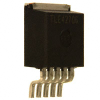
5-V Low Drop Voltage Regulator
TLE 7270
Features • • • • • • • Output voltage 5 V ±2% Ultra low current consumption: typ. 20µA 300 mA current capability Reset Feature Very low-drop voltage Short-circuit-proof Suitable for use in automotive electronics
P-TO252-5-1
Functional Description The TLE 7270 is a monolithic integrated low-drop voltage regulator which can supply loads up to 300 mA. An input voltage up to 42 V is regulated to VQ,nom = 5.0 V with a precision of ±2%. Due to its integrated reset circuitry featuring a 2-step adjustable power on timing and output voltage monitoring the IC is well suited for P-TO263-5-1 µ-controller supplies. The sophisticated design allows to achieve stable operation even with ceramic output capacitors down to 470 nF. The device is designed for the harsh environment of automotive applications. Therefore it is protected against overload, short circuit and overtemperature conditions. Of course the TLE 7270 can be used also in all other applications, where a stabilized 5 V voltage is required. Due to its ultra low current consumption the TLE 7270 is dedicated for use in applications permanently connected to VBAT. An integrated output sink current circuitry keeps the voltage at the Output pin Q below 5.5 V even when reverse currents are applied. Thus connected devices are protected from overvoltage damage. For applications requiring extremely low noise levels the Infineon voltage regulator family TLE 42XY and TLE 44XY is more suited than the TLE 7270. A mV-range output noise on the TLE 7270 caused by the charge pump operation is unavoidable due to the ultra low quiescent current concept. Type TLE 7270 D TLE 7270 G
Data Sheet
Ordering Code Q67006-A9670 on request
1
Package P-TO252-5-1 P-TO263-5-1
Rev. 1.03, 2004-10-14
�TLE 7270
Reset The Reset pin informs e.g. the microcontroller in case the output voltage has fallen below the lower threshold VRT of typ. 4.65 V. The hysteresis is typically 100mV. Connecting the regulator to a battery voltage at first the reset signal remains LOW. When the output voltage has reached the reset threshold VRT the reset output RO remains still LOW for the reset delay time trd adjustable in 2 steps via the DT Pin. Afterwards the reset output turns HIGH.
TLE 7270
I
1
5
Q
Overtemperature Shutdown Bandgap Reference
1
Reset Generator with Selectable Timing
2 4
RO DT
Charge Pump
3 GND
AEB03520.VSD
Figure 1
Block Diagram
Data Sheet
2
Rev. 1.03, 2004-10-14
�TLE 7270
GND
I RO
DT Q
AEP02825_7270
Figure 2 Table 1 1 2 I RO
Pin Configuration P-TO252-5-1 (D-PAK), P-TO263-5-1 (top view) Pin Definitions and Functions Input; block to ground directly at the IC with a ceramic capacitor. Reset Output. Open Collector Output with integrated pull-up resistor of typically 30kΩ. Optional external pull-up resistor of ≥ 10 kΩ to pin Q. Ground; Pin 3 internally connected to heatsink. Delay Time; connect to Q or GND to choose reset delay time. Output; block to ground with a ceramic capacitor, C ≥ 470 nF.
Pin No. Symbol Function
3 4 5
GND DT Q
Data Sheet
3
Rev. 1.03, 2004-10-14
�TLE 7270
Table 2 Parameter Input I Voltage Current Output Q Voltage Voltage Current
Absolute Maximum Ratings Symbol Limit Values Min. Max. 45 – 5.5 6.2 – 5.5 6.2 1 5.5 6.2 1 150 150 V mA V V mA V V mA V V mA °C °C – – – Unit Test Condition
VI II VQ VQ IQ VRO VRO IRO VDT VDT IDT Tj Tstg
-0.3 -1 -0.3 -0.3 -1 -0.3 -0.3 -1 -0.3 -0.3 -1 -40 -50
t < 10 s1)
– –
Reset Output RO Voltage Voltage Current Delay Time DT Voltage Voltage Current Temperature Junction temperature Storage temperature – – –
t < 10 s1)
–
t < 10 s1)
–
1) Exposure to these absolute maximum ratings for extended periods (t > 10 s) may affect device reliability.
Note: Stresses above those listed here may cause permanent damage to the device. Exposure to absolute maximum rating conditions for extended periods may affect device reliability. Table 3 Parameter Input voltage Junction temperature Operating Range Symbol Limit Values Min. Max. 42 150 V °C – – 5.5 -40 Unit Remarks
VI Tj
Note: In the operating range, the functions given in the circuit description are fulfilled.
Data Sheet
4
Rev. 1.03, 2004-10-14
�TLE 7270
Table 4 Parameter Junction case
Thermal Resistance Symbol Limit Values Min. Max. 101) 801) 551) K/W – K/W TO2522) K/W TO2633) × 80 × 1.5 mm3, heat sink × 80 × 1.5 mm3, heat sink – – – Unit Remarks
Junction ambient Junction ambient
Rthj-c Rthj-a Rthj-a
1) Target values need to be verified 2) Worst case, regarding peak temperature; zero airflow; mounted on a PCB FR4, 80 area 300 mm2 3) Worst case, regarding peak temperature; zero airflow; mounted on a PCB FR4, 80 area 300 mm2
Table 5
Electrical Characteristics
VI = 13.5 V; – 40 °C < Tj < 150 °C (unless otherwise specified)
Parameter Output Q Output voltage Output voltage Symbol Limit Values Min. Typ. Max. 5.0 5.0 – 20 – 200 15 5 5.1 5.1 – 800 – – – – 40 – 20 30 40 500 40 20 Unit Measuring Condition
VQ VQ
4.9 4.9 320
V V
mA mA µA µA mV mV mV
0.1 mA
很抱歉,暂时无法提供与“TLE7270G”相匹配的价格&库存,您可以联系我们找货
免费人工找货