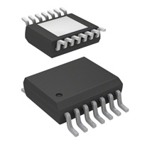
0
登录后你可以
  • 下载海量资料
  • 学习在线课程
  • 观看技术视频
  • 写文章/发帖/加入社区
创作中心
发布
  • 发文章

  • 发资料

  • 发帖

  • 提问

  • 发视频

创作活动
TLE7272-2E

TLE7272-2E

  • 厂商:

    INFINEON

  • 封装:

  • 描述:

    TLE7272-2E - 5-V Low Dropout Voltage Regulator - Infineon Technologies AG

  • 数据手册
  • 价格&库存
TLE7272-2E 数据手册
Data Sheet, Rev. 1.0, June 2009 TLE7272-2 5-V Low Dropout Voltage Regulator Automotive Power 5-V Low Dropout Voltage Regulator TLE7272-2 1 Features • • • • • • • • • • • • Overview Ultra Low Current Consumption 20 µA Output Voltage 5 V ±2% Output Current up to 300 mA Power-On and Undervoltage Reset Reset Low Down to VQ = 1 V Enable Input Very Low Dropout Voltage Output Current Limitation Overtemperature Shutdown Wide Temperature Range From -40 °C up to 150 °C Green Product (RoHS compliant) AEC Qualified PG-SSOP-14 Exposed Pad Description The TLE7272-2 is a monolithic integrated low dropout voltage regulator for load currents up to 300 mA. An input voltage up to 42 V is regulated to VQ,nom = 5.0 V with a precision of ±2%. Due to its integrated reset circuitry featuring power on timing and output voltage monitoring the IC is well suited as µ-controller supply. The sophisticated design allows to PG-TO252-5 achieve stable operation even with ceramic output capacitors down to 470 nF. The device is designed for the harsh environment of automotive applications. Therefore it is protected against overload, short circuit and overtemperature conditions by the implemented output current limitation and the overtemperature shutdown circuit. The TLE7272-2 can be also used in all other applications requiring a stabilized 5 V voltage. Due to its ultra low quiescent current of typically 20 µA the TLE7272-2 is dedicated for use in applications permanently connected to VBAT. In addition the device can be switched off via the Enable input reducing the current consumption to typically 5 µA. An integrated output sink current circuitry keeps the voltage at the Output pin Q below 5.5 V even in case of occuring reverse currents. Thus connected devices are protected from overvoltage damage. For applications requiring extremely low noise levels the Infineon voltage regulator family TLE 42XX and TLE 44XX is more suited than the TLE7272-2. A mV-range output noise on the TLE7272-2 caused by the charge pump operation is unavoidable due to the ultra low quiescent current concept. Type TLE7272-2E TLE7272-2D Data Sheet Package PG-SSOP-14 Exposed Pad PG-TO252-5 2 Marking 7272-2E 7272-2D Rev. 1.0, 2009-06-01 TLE7272-2 Block Diagram 2 Block Diagram TLE7272-2 I Overtemperature Shutdown Bandgap Reference Q Reset Generator RO 1 EN Enable Charge Pump GND AEB03523.VSD Figure 1 Block Diagram Data Sheet 3 Rev. 1.0, 2009-06-01 TLE7272-2 Pin Configuration 3 3.1 Pin Configuration Pin Assignment PG-SSOP-14 Exposed Pad Figure 2 Pin Configuration (top view) 3.2 Pin No. 1,3,5,7 2 Pin Definitions and Functions PG-SSOP-14 Exposed Pad Symbol Function n.c. RO non connected can be open or connected to GND Reset Output open collector output with integrated pull-up resistor; optional external pull-up resistor of ≥ 10 kΩ to pin Q; leave open if reset function not needed Ground Enable Input high level input signal enables the IC; low level input signal disables the IC; integrated pull-down resistor non connected can be open or connected to GND Output block to ground with a capacitor close to the IC terminals, respecting the values given for its capacitance and ESR in “Functional Range” on Page 6 Input block to ground directly at the IC with a ceramic capacitor Exposed Pad connect to GND and heatsink area 4 6 GND EN 8,10,11,12,14 9 n.c. Q 13 Pad I – Data Sheet 4 Rev. 1.0, 2009-06-01 TLE7272-2 Pin Configuration 3.3 Pin Assignment PG-TO252-5 GND I RO EN Q Figure 3 Pin Configuration (top view) 3.4 Pin No. 1 2 Pin Definitions and Functions PG-TO252-5 Symbol Function I RO Input block to ground directly at the IC with a ceramic capacitor Reset Output open collector output with integrated pull-up resistor; optional external pull-up resistor of ≥ 10 kΩ to pin Q; leave open if reset function not needed Ground internally connected to heat slug Enable Input high level input signal enables the IC; low level input signal disables the IC; integrated pull-down resistor Output block to ground with a capacitor close to the IC terminals, respecting the values given for its capacitance and ESR in “Functional Range” on Page 6 Heat Slug internally connected to GND; connect to GND and heatsink area 3 4 GND EN 5 Q Heat Slug – Data Sheet 5 Rev. 1.0, 2009-06-01 TLE7272-2 General Product Characteristics 4 4.1 General Product Characteristics Absolute Maximum Ratings Absolute Maximum Ratings1) Tj = -40 °C to 150 °C; all voltages with respect to ground, (unless otherwise specified) Pos. Input I 4.1.1 4.1.2 4.1.3 4.1.4 4.1.5 4.1.6 4.1.7 4.1.8 1) 2) 3) 4) Parameter Symbol Min. Limit Values Max. 45 6 6.2 45 150 150 3 1.5 Unit Test Condition Voltage Voltage Voltage Voltage Junction temperature Storage temperature Human Body Model (HBM)3) Charged Device Model (CDM) 4) VI VQ, VRO VQ, VRO VEN Tj Tstg Voltage Voltage -0.3 -0.3 -0.3 -0.3 -40 -50 - V V V V °C °C kV kV – – Output Q, Reset Output RO t < 10 s2) – – – – – Enable Input EN Temperature ESD Susceptibility not subject to production test, specified by design exposure to these absolute maximum ratings for extended periods (t > 10 s) may affect device reliability ESD susceptibility Human Body Model “HBM” according to AEC-Q100-002 - JESD22-A114 ESD susceptibility Charged Device Model “CDM” according to ESDA STM5.3.1 Note: Stresses above the ones listed here may cause permanent damage to the device. Exposure to absolute maximum rating conditions for extended periods may affect device reliability. Note: Integrated protection functions are designed to prevent IC destruction under fault conditions described in the data sheet. Fault conditions are considered as “outside” normal operating range. Protection functions are not designed for continuous repetitive operation. 4.2 Pos. 4.2.1 4.2.2 4.2.3 4.2.4 Functional Range Parameter Input voltage Output Capacitor’s Requirements Junction temperature Symbol Limit Values Min. Max. 42 – 10 150 V nF Ω °C – 1) 2) Unit Remarks VI CQ ESR(CQ) Tj 5.5 470 – -40 – 1) the minimum output capacitance requirement is applicable for a worst case capacitance tolerance of 30% 2) relevant ESR value at f = 10 kHz Note: Within the functional or operating range, the IC operates as described in the circuit description. The electrical characteristics are specified within the conditions given in the Electrical Characteristics table. Data Sheet 6 Rev. 1.0, 2009-06-01 TLE7272-2 General Product Characteristics 4.3 Thermal Resistance Note: This thermal data was generated in accordance with JEDEC JESD51 standards. For more information, go to www.jedec.org. Pos. Parameter Symbol Min. TLE7272-2E (PG-SSOP-14 Exposed Pad) 4.3.1 4.3.2 4.3.3 4.3.4 4.3.5 TLE7272-2D (PG-TO252-5) 4.3.1 4.3.2 4.3.3 4.3.4 4.3.5 Junction to Case1) Junction to Ambient1) Junction to Case1) Junction to Ambient1) Limit Values Typ. 14 47 141 66 56 Max. – – – – – K/W K/W K/W K/W K/W measured to exposed pad 2) Unit Conditions RthJC RthJA RthJA RthJA RthJA – – – – – footprint only3) 300 mm² heatsink area3) 600 mm² heatsink area3) measured to tab 2) RthJC RthJA RthJA RthJA RthJA – – – – – 6 32 115 62 47 – – – – – K/W K/W K/W K/W K/W footprint only3) 300 mm² heatsink area3) 600 mm² heatsink area3) 1) Not subject to production test, specified by design. 2) Specified RthJA value is according to Jedec JESD51-2,-5,-7 at natural convection on FR4 2s2p board; The Product (Chip+Package) was simulated on a 76.2 x 114.3 x 1.5 mm³ board with 2 inner copper layers (2 x 70µm Cu, 2 x 35µm Cu). Where applicable a thermal via array under the exposed pad contacted the first inner copper layer. 3) Specified RthJA value is according to Jedec JESD 51-3 at natural convection on FR4 1s0p board; The Product (Chip+Package) was simulated on a 76.2 × 114.3 × 1.5 mm3 board with 1 copper layer (1 x 70µm Cu). Data Sheet 7 Rev. 1.0, 2009-06-01 TLE7272-2 Electrical Characteristics 5 5.1 Electrical Characteristics Electrical Characteristics Voltage Regulator Electrical Characteristics VI =13.5 V; Tj = -40 °C to 150 °C; all voltages with respect to ground (unless otherwise specified) Pos. Parameter Symbol Limit Values Min. Output Q 5.1.1 5.1.2 5.1.3 5.1.4 5.1.5 5.1.6 5.1.7 5.1.8 5.1.9 Output Voltage Output Voltage Dropout Voltage Load Regulation Line Regulation Output Current Limitation Output Current Limitation Power Supply Ripple Rejection2) Temperature Output Voltage Drift Typ. 5.0 5.0 250 15 5 – – 60 0.5 Max. 5.1 5.1 500 40 20 – 800 – – V V mV mV mV mA mA dB mV/K 0.1 mA < IQ
TLE7272-2E 价格&库存

很抱歉,暂时无法提供与“TLE7272-2E”相匹配的价格&库存,您可以联系我们找货

免费人工找货