Door Module Power IC TLE 8201R
Data Sheet Rev. 2.0
Features • Full bridge (150mΩ) for main doorlock motor • Two half-bridges (400mΩ) for deadbolt and mirror position motor or mirror fold motor • Two half-bridges (800mΩ) for mirror position • High-side switch (100mΩ) for mirror defrost • Four high-side switches (500mΩ) for 5W and 10W lamps • Current sense analog output with multiplex • All outputs with short circuit protection and diagnosis • Over-temperature protection with warning • Open load diagnosis for all outputs • Charge pump-Output for n-channel MOS-FET reverse-polarity protection • Very low current consumption in sleep mode • Standard 16-bit SPI for control and diagnosis • Over-and Undervoltage Lockout • Power-SO package with full-size heatslug for excellent low thermal resistance Type TLE 8201R Functional Description The TLE 8201R is an Application Specific Standard Product for automotive door-module applications. It includes all the power stages necessary to drive the loads in a typical front door application, i.e. central lock, deadlock or mirror fold, mirror position, mirror defrost and 5W or 10W lamps, e.g for turn signal, courtesy/warning or control panel illumination. It is designed as a monolithic circuit in Infineons mixed technology SPT which combines bipolar and CMOS control circuitry with DMOS power devices. Short circuit and over-temperature protection and a detailed diagnosis are in line with the safety requirements of automotive applications. The current sense output allows to improve the total system performance. The standard SPI interface saves microcontroller I/O lines while still giving flexible control of the power stages and a detailed diagnosis. Ordering Code Package/Shipment PG-DSO-36-27
Data Sheet Rev. 2.0
1
2006-06-07
�TLE 8201R
Table of Contents 1 2 2.1 2.2 3 3.1 3.2 3.3 4 4.1 4.1.1 4.1.2 4.1.3 4.1.4 4.2 4.2.1 4.2.2 4.2.3 4.3 4.3.1 4.3.2 4.3.3 4.3.4 4.3.5 4.3.6 4.4 4.4.1 4.4.2 4.5 4.5.1 4.5.2 4.6 4.6.1 4.6.2 4.7 4.7.1 5 6
Page
Block Diagram . . . . . . . . . . . . . . . . . . . . . . . . . . . . . . . . . . . . . . . . . . . . . . 3 Pin Configuration . . . . . . . . . . . . . . . . . . . . . . . . . . . . . . . . . . . . . . . . . . . . 4 Pin Assignment . . . . . . . . . . . . . . . . . . . . . . . . . . . . . . . . . . . . . . . . . . . . . 4 Pin Definitions and Functions . . . . . . . . . . . . . . . . . . . . . . . . . . . . . . . . . . . 5 Electrical Characteristics . . . . . . . . . . . . . . . . . . . . . . . . . . . . . . . . . . . . . Absolute Maximum Ratings . . . . . . . . . . . . . . . . . . . . . . . . . . . . . . . . . . . . . Operating Range . . . . . . . . . . . . . . . . . . . . . . . . . . . . . . . . . . . . . . . . . . . . . Thermal Resistance . . . . . . . . . . . . . . . . . . . . . . . . . . . . . . . . . . . . . . . . . . . 7 7 8 8
Block Description and Electrical Characteristics . . . . . . . . . . . . . . . . . . 9 Power Supply . . . . . . . . . . . . . . . . . . . . . . . . . . . . . . . . . . . . . . . . . . . . . . . . 9 General . . . . . . . . . . . . . . . . . . . . . . . . . . . . . . . . . . . . . . . . . . . . . . . . . . 9 Sleep-Mode . . . . . . . . . . . . . . . . . . . . . . . . . . . . . . . . . . . . . . . . . . . . . . . 9 Reverse Polarity . . . . . . . . . . . . . . . . . . . . . . . . . . . . . . . . . . . . . . . . . . . 9 Electrical Characteristics . . . . . . . . . . . . . . . . . . . . . . . . . . . . . . . . . . . . . 9 Monitoring Functions . . . . . . . . . . . . . . . . . . . . . . . . . . . . . . . . . . . . . . . . . 11 Power Supply Monitoring . . . . . . . . . . . . . . . . . . . . . . . . . . . . . . . . . . . . 11 Temperature Monitoring . . . . . . . . . . . . . . . . . . . . . . . . . . . . . . . . . . . . 12 Current Sense . . . . . . . . . . . . . . . . . . . . . . . . . . . . . . . . . . . . . . . . . . . . 13 SPI . . . . . . . . . . . . . . . . . . . . . . . . . . . . . . . . . . . . . . . . . . . . . . . . . . . . . . . 14 General . . . . . . . . . . . . . . . . . . . . . . . . . . . . . . . . . . . . . . . . . . . . . . . . . 14 Register Address . . . . . . . . . . . . . . . . . . . . . . . . . . . . . . . . . . . . . . . . . . 14 SPI bit definitions . . . . . . . . . . . . . . . . . . . . . . . . . . . . . . . . . . . . . . . . . . 16 Status Register Address selection and Reset . . . . . . . . . . . . . . . . . . . . 20 Electrical Characteristics . . . . . . . . . . . . . . . . . . . . . . . . . . . . . . . . . . . . 21 PWM inputs . . . . . . . . . . . . . . . . . . . . . . . . . . . . . . . . . . . . . . . . . . . . . . 22 Power-Outputs 1-6 (Bridge Outputs) . . . . . . . . . . . . . . . . . . . . . . . . . . . . . 25 Protection and Diagnosis . . . . . . . . . . . . . . . . . . . . . . . . . . . . . . . . . . . . 25 Electrical Characteristics . . . . . . . . . . . . . . . . . . . . . . . . . . . . . . . . . . . . 27 Power-Output 7 (Mirror heater driver) . . . . . . . . . . . . . . . . . . . . . . . . . . . . 31 Protection and Diagnosis . . . . . . . . . . . . . . . . . . . . . . . . . . . . . . . . . . . . 31 Electrical Characteristics . . . . . . . . . . . . . . . . . . . . . . . . . . . . . . . . . . . . 33 Power-Outputs 8 - 11 (Lamp drivers) . . . . . . . . . . . . . . . . . . . . . . . . . . . . 35 Protection and Diagnosis . . . . . . . . . . . . . . . . . . . . . . . . . . . . . . . . . . . . 35 Electrical Characteristics . . . . . . . . . . . . . . . . . . . . . . . . . . . . . . . . . . . . 38 Logic In- and Outputs . . . . . . . . . . . . . . . . . . . . . . . . . . . . . . . . . . . . . . . . 40 Electrical Characteristics . . . . . . . . . . . . . . . . . . . . . . . . . . . . . . . . . . . . 40 Application Description . . . . . . . . . . . . . . . . . . . . . . . . . . . . . . . . . . . . . 41 Package Outlines . . . . . . . . . . . . . . . . . . . . . . . . . . . . . . . . . . . . . . . . . . 43
Data Sheet Rev. 2.0
2
2006-06-07
�TLE 8201R
Block Diagram
1
Block Diagram
Vs
GO CP Chargepump RevPol MOS driver FaultDetect
Vcc INH CSN CLK DI DO PWM1 PWM2 ISO
Biasing
OUT1
OUT2
SPI OUT3 Logic and Latch
Logic IN current sense MUX
OUT4
OUT5 OUT8 OUT9 OUT10 OUT11 GND OUT7 OUT6
Figure 1
Block Diagram
Data Sheet Rev. 2.0
3
2006-06-07
�TLE 8201R
Pin Configuration
2
2.1
Pin Configuration
Pin Assignment
cooling tab (GND)
GND OUT5 OUT6 Vs INH PWM1 PWM2 ISO Vcc DO CLK CSN DI GO Vs OUT1 OUT1 GND
1 2 3 4 5 6 7 8 9 10 11 12 13 14 15 16 17 18
36 35 34 33 32 31 30 29 28 27 26 25 24 23 22 21 20 19
GND n.c. OUT4 Vs OUT7 OUT7 Vs OUT8 OUT9 CP Vs OUT10 OUT11 Vs OUT3 OUT2 OUT2 GND
Figure 2
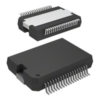
Pin Configuration PG-DSO-36-27
Data Sheet Rev. 2.0
4
2006-06-07
�TLE 8201R
Pin Configuration
2.2
Pin cooling tab 1, 18, 19, 36 2 3
Pin Definitions and Functions
Symbol GND GND OUT5 OUT6 Function Cooling tab, internally connected to GND; to reduce thermal resistance place cooling areas and thermal vias on PCB. Ground; internally connected to cooling tab (heat slug). Power-Output of half-bridge 5; DMOS half-bridge Power-Output of half-bridge 6; DMOS half-bridge. Power supply; needs decoupling capacitors to GND. > 47µF electrolytic in parallel with 100nF ceramic is recommended. All Vs pins must be connected externally Inhibit; active low. Sets the device in sleep mode with low current consumption when left open or pulled to LOW. Has an internal pull down current source Logic Input for direct power stage control; direct input to control the high-side switches selected by the SPI xsel1 bits in control register CtrlReg01 Logic Input for direct power stage control; direct input to control the switches selected by the SPI xsel2 bits in control register CtrlReg11 Current sense output; Mirrors the current of the high-side switch selected by the current sense multiplexer control bits ISx Logic Supply Voltage; needs decoupling capacitors to GND (pin 1). 10µF electrolytic in parallel with 10nF ceramic is recommended Serial Data Output; Transfers data to the master when the chip is selected by CSN=LOW. Data transmission is synchronized by CLK, DO state is changed on the rising edge of CLK. The most significant bit (MSB) is transferred first. The pin is tristated as long as CSN=HIGH Serial Data Clock Input; Receives the clock signal from the master and clocks the SPI shift register. Has an internal pull down current source Serial Port Chip Select Not Input; SPI communication is enabled by pulling CSN to LOW. CLK must be LOW during the transition of CSN. The CSN-pin has an internal pull-up current source
5 2006-06-07
4, 15, 23, Vs 26, 30, 33 5 INH
6
PWM1
7
PWM2
8 9
ISO Vcc
10
DO
11
CLK
12
CSN
Data Sheet Rev. 2.0
�TLE 8201R
Pin Configuration Pin 13 Symbol DI Function Serial Data Input; Receives serial data from the master when the chip is selected by CSN=LOW. Data transmission is synchronized by CLK. Data are accepted on the falling edge of CLK. The LSB is transferred first. The DI-pin has an internal pulldown current source. Gate Out; Charge pump output to drive the gate of external nchannel MOS-FET for reverse polarity protection Power-Output of half-bridge 1; DMOS half-bridge. Power-Output of half-bridge 2; DMOS half-bridge. Power-Output of half-bridge 3; DMOS half-bridge Power Output of high-side switch 11; DMOS high-side switch Power Output of high-side switch 10; DMOS high-side switch Charge Pump; pin for optional external charge-pump reservoir capacitor. 3.3 nF to Vs is recommended Power-Output of high-side switch 9; DMOS high-side switch Power-Output of high-side switch 8; DMOS high-side switch Power Output of high-side switch 7; DMOS high-side switch Power-Output of half-bridge 4; DMOS half-bridge Not connected
14 16, 17 20, 21 22 24 25 27 28 29 31, 32 34 35
GO OUT1 OUT2 OUT3 OUT11 OUT10 CP OUT9 OUT8 OUT7 OUT4 n.c.
Data Sheet Rev. 2.0
6
2006-06-07
�TLE 8201R
Electrical Characteristics
3
3.1
Pos. 3.1.1 3.1.2 3.1.3 3.1.4 3.1.5 3.1.6 3.1.7
Electrical Characteristics
Absolute Maximum Ratings
Parameter Supply voltage Logic supply Voltage Logic input- and output Voltages Voltage at GO-pin Symbol Limit Values Unit Remarks min. max. 40 5.5 5.5 V V V – – – – – – Human Body Model according to ANSI EOS\ESD S5.1 standard (eqv. to MIL STD 883D and JEDEC JESD22A114) -0.3 -0.3 -0.3 -16 -40 -50 –
VS VCC
VGO Junction temperature Tj Storage temperature Tstg ESD capability of power VESD stage output and VS
ESD capability of logic pins and ISO pin
VS + 5 V
150 150 4 °C °C kV
pins 3.1.8
VESD
–
2
kV
Note: Stresses above the ones listed here may cause permanent damage to the device. Exposure to absolute maximum rating conditions for extended periods may affect device reliability. Note: Integrated protection functions are designed to prevent IC destruction under fault conditions described in the data sheet. Fault conditions are considered as “outside” normal operating range. Protection functions are not designed for continuous repetitive operation.
Data Sheet Rev. 2.0
7
2006-06-07
�TLE 8201R
Electrical Characteristics
3.2
Pos. 3.2.1 3.2.2 3.2.3 3.2.4 3.2.5 3.2.6
Operating Range
Parameter Supply voltage Supply voltage Supply voltage Logic supply voltage SPI clock frequency Junction temperature Symbol Limit Values min. max. 40 20 20 5.5 2 150 V V V V MHz °C Including overvoltage lockout Functional Parameter Specification – – – 5 5 8 4.75 – -40 Unit Remarks
VS VS VS VCC fCLK Tj
Note: Within the functional range the IC operates as described in the circuit description. The electrical characteristics are specified within the limit given at the table.
3.3
Pos. 3.3.1 3.3.2
Thermal Resistance
Parameter Junction pin Junction ambient Symbol Limit Values Unit min. max. 1.5 50 K/W K/W – minimal footprint – – Conditions
RthjC RthjA
Data Sheet Rev. 2.0
8
2006-06-07
�TLE 8201R
Block Description and Electrical Characteristics
4
4.1 4.1.1
Block Description and Electrical Characteristics
Power Supply General
The TLE 8201R has two power supply inputs: All power drivers are connected to the supply voltage VS which is connected to the automotive 12 V board-net. The internal logic part is supplied by a separate Voltage VCC = 5 V. The advantage of this system is that information stored in the logic remains intact in the event of short-term failures in the supply voltage VS. The system can therefore continue to operate after VS has recovered, without having to be reprogrammed. A rising edge on VCC triggers an internal Power-On Reset (POR) to initialize the IC at power-on. All data stored internally is deleted, and the outputs are switched to highimpedance status (tristate).
4.1.2
Sleep-Mode
The TLE 8201R can be put in a low current-consumtion mode by setting the input INH to LOW. The INH pin has an internal pull-down current source. In sleep-mode, all output transistors are turned off and the SPI is not operating. When enabling the IC by setting INH from L to H, a Power-On Reset is performed as described above.
4.1.3
Reverse Polarity
The TLE 8201R requires an external reverse polarity protection. The gate-driver (charge-pump output) for an external n-channel logic-level MOS-FET is integrated. The gate voltage is provided at pin GO which should be connected as shown in the application diagram.
4.1.4
Electrical Characteristics
Electrical Characteristics 8 V < VS < 20 V; 4.75 V < VCC < 5.25 V; INH = High; all outputs open; -40 °C < Tj < 150 °C; unless otherwise specified Pos. Parameter Symbol Limit Values min. typ. max. Unit Conditions
Current Consumption 4.1.1 4.1.2 Supply current Logic supply current
IS ICC
9
– –
3.0 5
7.0 10
mA mA
– SPI not active
2006-06-07
Data Sheet Rev. 2.0
�TLE 8201R
Block Description and Electrical Characteristics Electrical Characteristics 8 V < VS < 20 V; 4.75 V < VCC < 5.25 V; INH = High; all outputs open; -40 °C < Tj < 150 °C; unless otherwise specified Pos. 4.1.3 4.1.4 4.1.5 Parameter Quiescent current Logic quiescent current Total quiescent current Symbol
IS ICC
Limit Values min. – – typ. 2.5 0.2 3 max. 5 1 6
Unit Conditions µA µA µA INH = L, VS = 14 V, VOUT7-11 = 0V; Tj < 85 °C
IGO = 50 µA
IS + Icc –
Charge Pump-output for Reverse-Polarity Protection FET (GO) 4.1.6 4.1.7 4.1.8 Gate-Voltage Setup-time Reverse leakage current
VGO VS tGO IlkGO
5 – –
– – –
8 1 5
V ms µA
–
VS = 0 V VGO = -14 V
Data Sheet Rev. 2.0
10
2006-06-07
�TLE 8201R
4.2 4.2.1
Monitoring Functions Power Supply Monitoring
The power supply Voltage VS is monitored for over- and under voltage. • Under Voltage If the supply voltage VS drops below the switch off voltage VUV OFF, all output transistors are switched off and the power supply fail bit PSF is set. The error is not latched, i.e. if VS rises again and reaches the switch on voltage VUV ON, the power stages are restarted and the error bit is reset. • Over Voltage If the supply voltage VS rises above the switch off voltage VOV OFF, all output transistors are switched off and the power supply fail bit (bit 7 of the SPI diagnosis word) is set. The error is not latched, i.e. if VS falls again and reaches the switch on voltage VOV ON, the power stages are restarted and the error is reset.
4.2.1.1
Characteristics Power Supply Monitoring
Electrical Characteristics 8 V < VS < 20 V; 4.75 V < VCC < 5.25 V; INH = High; all outputs open; -40 °C < Tj < 150 °C; unless otherwise specified Pos. Parameter
4.2.1 4.2.2 4.2.3 4.2.4 4.2.5 4.2.6 UV-Switch-ON voltage UV-Switch-OFF voltage UV-ON/OFF-Hysteresis OV-Switch-OFF voltage OV-Switch-ON voltage OV-ON/OFF-Hysteresis
Symbol
VUVON VUVHY VOVOF
F
Limit Values min.
– – 21 20 0.5
Unit Conditions
V V V V V V
typ.
– – 0.25 – – 1
max.
5.2 5.0 – 25 24 –
VS increasing VS decreasing VUVON - VUVOFF VS increasing VS decreasing VOVOFF VOVON
VUVOFF 4.0
VOVON VOVHY
Data Sheet Rev. 2.0
11
2006-06-07
�TLE 8201R
4.2.2
Temperature Monitoring
Temperature sensors are integrated in the power stages. The temperature monitoring circuit compares the measured temperature to the warning and shutdown thresholds. If one or more temperature sensors reach the warning temperature, the temperature warning bit TW is set to HIGH. This bit is not latched (i.e. if the temperature falls below the warning threshold (with hysteresis), the TW bit is reset to LOW again). If one or more temperature sensors reach the shut-down temperature, the outputs are shut down as described in the next paragraph and the temperature shut-down bit TSD is set to HIGH. The shutdown is latched (i.e. the output stages remain off and the TSD bit set high until a SRR command is sent or a power-on reset is performed). The power-stages are subdivided into two groups for over-temperature shut-down: • Group1: OUT 1, OUT 2 and OUT 3 • Group2: OUT 4 to 11 If one or more temperature sensors within a group reaches the shutdown threshold, all outputs within the group are switched off, while the other outputs continue normal operation.
4.2.2.1
Characteristics Temperature Monitoring
Electrical Characteristics 8 V < VS < 20 V; 4.75 V < VCC < 5.25 V; INH = High; all outputs open; -40 °C < Tj < 150 °C; unless otherwise specified Pos. Parameter
4.2.7 4.2.8 4.2.9 Thermal warning junction temperature1) Temperature warning hysteresis1) Thermal shutdown junction temperature1)
Symbol
TjW
∆T
Limit Values min.
120 – 150 120 – 1.05
Unit Conditions
°C K °C °C K – – – – – – –
typ.
145 30 175 – 30 1.20
max.
170 – 200 170 – –
TjSD TjSO
∆T
4.2.10 Thermal switch-on junction temperature1) 4.2.11 Temperature shutdown hysteresis1)
4.2.12 Ratio of SD to W temperature1) TjSD /
TjW
1)
Not subject to production test, specified by design
Data Sheet Rev. 2.0
12
2006-06-07
�TLE 8201R
4.2.3
Current Sense
A current proportional to the output current that flows from the selected power output to GND is provided at the ISO (I sense out) pin. The output selection is done via the SPI. The sense current can be transformed into a voltage by an external sense resistor and provided to an A/D converter input (see section application).
4.2.3.1
Characteristics Current Sense
Electrical Characteristics 8 V < VS < 20 V; 4.75 V < VCC < 5.25 V; INH = High; all outputs open; -40 °C < Tj < 150 °C; unless otherwise specified Pos. Parameter
HS1, HS2 (Register IS = 000, 001) 4.2.13 Output voltage range 4.2.14 Current Sense Ratio 4.2.15 Current Sense accuracy 4.2.16 Matching HS3, HS4 (Register IS = 010, 011) 4.2.17 Output voltage range 4.2.18 Current Sense Ratio 4.2.19 Current Sense accuracy HS7 (Register IS = 100) 4.2.20 Output voltage range 4.2.21 Current Sense Ratio for HS7 4.2.22 Current Sense accuracy
Symbol
VISO12 kILIS12
12
Limit Values min.
0 –
Unit Conditions
typ.
– 2000 – 1
max.
3 – 10 2 V – % %
VCC = 5 V kILIS = IOUT/IISO IOUT > 3 A
∆kILIS12 = (kILIS1 - kILIS2) / kILIS1
kILISacc –
∆kILIS1
2
-6
VISO34 kILIS34
0 –
– 1000 – – 2000 –
3 – 10 3 – 10
V – % V – %
VCC = 5 V kILIS = IOUT/IISO IOUT > 1.5 A VCC = 5 V kILIS = IOUT/IISO IOUT > 2A
kILISacc – VISO7 kILIS7
0 –
kILISacc –
Data Sheet Rev. 2.0
13
2006-06-07
�TLE 8201R
4.3 4.3.1
SPI General
The SPI is used for bidirectional communication with a control unit. The TLE 8201R acts as SPI-slave and the control unit acts as SPI-master. The 16-bit control word is read via the DI serial data input. The status word appears synchronously at the DO serial data output. The communication is synchronized by the serial clock input CLK. Standard data transfer timing is shown in Figure 3. The clock polarity is data valid on falling edge. CLK must be low during CSN transition. The transfer is MSB first. The transmission cycle begins when the chip is selected with the chip-select-not (CSN) input (H to L). Then the data is clocked through the shift register. The transmission ends when the CSN input changes from L to H and the word which has been read into the shift register becomes the control word. The DO output switches then to tristate status, thereby releasing the DO bus circuit for other uses. The SPI allows to parallel multiple SPI devices by using multiple CSN lines. The SPI can also be used with other SPIdevices in a daisy-chain configuration.
CSN High to Low & rising edge of SCLK: SDO is enabled. Status information is transfered to Output Shift Register CSN CSN Low to High: Data from Shift-Register is transfered to Output Driver Logic CLK 15 14 13 12 11 10 9 8 7 6 5 4 3 2 1 0 15 14
time
actual Data DI 15 14 13 12 11 10 9 8 7 6 5 4 3 2 1 0
new Data 15 14
SDI: Data will be accepted on the falling edge of CLK-Signal previous Status DO EF 15 14 13 12 11 10 9 8 7 6 5 4 3 2 10 actual Status 15 14
SDO: State will change on the rising edge of CLK-Signal
Figure 3
SPI standard data transfer timing
4.3.2
Register Address
The 16-bit SPI frame is composed of an addressable block, an address-independent block and a 2-bit address as shown in Figure 4. The control word transmitted from the master to the TLE 7201R is executed at the end of the SPI transmission (CSN L -> H) and remains valid until a different control word is transmitted or a power on reset occurs. At the beginning of the SPI transmission (CSN
Data Sheet Rev. 2.0
14
2006-06-07
�TLE 8201R
H ->L), the diagnostic data currently valid are latched into the SPI and transferred to the master. For Status Register address handling, please refer to Section 4.3.4
CSN time bit 15 14 13 12 11 10 9 8 7 6 5 4 3 2 1 0
DI
Input data Data for selected register address output data Data from selected register address
generic data
Register Address
DO
generic data
Figure 4
SPI structure
Data Sheet Rev. 2.0
15
2006-06-07
�TLE 8201R
4.3.3 4.3.3.1
Table 1 Bit
SPI bit definitions Control - word
Input (Control) Data Register CtrlReg 01 PWM1 input select HS7sel1 HS8sel1 HS9sel1 HS10sel1 HS11sel1 LS1sel1 LS2sel1 LS3sel1 OpL7ON Testmode IS_2 IS_1 IS_0 SRR RA_1 = 0 RA_0 = 1 CtrlReg 10 CtrlReg 11 Mirror and Lamp- PWM2 input driver control select LS4ON HS4ON LS5ON HS5ON LS6ON HS6ON HS8ON HS9ON HS10ON HS11ON IS_2 IS_1 IS_0 SRR Address - bits RA_1 = 1 RA_0 = 0 HS7sel2 HS8sel2 HS9sel2 HS10sel2 HS11sel2 LS1sel2 LS2sel2 LS3sel2 OpL89ON OpL1011ON IS_2 IS_1 IS_0 SRR RA_1 = 1 RA_0 = 1
CtrlReg 00 Lock and Mirror heat control LS1ON HS1ON LS2ON HS2ON LS3ON HS3ON HS7ON Testmode Testmode Testmode IS_2 IS_1 IS_0 SRR RA_1 = 0 RA_0 = 0
15 14 13 12 11 10 9 8 7 6 5 4 3 2 1 0
Address - independent data
Note: Testmode-bits must be set to L for normal operation
Data Sheet Rev. 2.0
16
2006-06-07
�TLE 8201R
Table 2 Control Bit LSxON HSxON xsel1 xsel2 OpL7ON OpL89ON OpL1011ON IS_x
Control bit definitions Definition low-side switch no. x is turned ON (OFF) if this bit is set to HIGH (LOW) high-side switch no. x is turned ON (OFF) if this bit is set to HIGH (LOW) power switch x is selected to be switched by the PWM1 input. power switch x is selected to be switched by the PWM2 input the pull-up current for open-load detection on output 7 is switched on (off) if this bit is set to HIGH (LOW) the pull-up currents for open-load detection on outputs 8 and 9 are switched on (off) if this bit is set to HIGH (LOW) the pull-up currents for open-load detection on outputs 10 and 11are switched on (off) if this bit is set to HIGH (LOW) the output for the current sense multiplexer is selected by these bits: IS_2 0 0 0 0 1 IS_1 0 0 1 1 0 IS_0 0 1 0 1 0 Power stage selected for current sense HS1 HS2 HS3 HS4 HS7 no output selected (IISO = 0)
all others SRR
Status Register Reset. If set to high, the error bits of the selected status register are reset after transmission of the data in the next SPI frame (see Section 4.3.4) Register Address, selects the control-register address for the current SPI transmission and the status-register address for the next SPI transmission
RA_x
Data Sheet Rev. 2.0
17
2006-06-07
�TLE 8201R
4.3.3.2
Table 3 Bit
Diagnosis
Output (Status) Data Register StatReg 01 Lock and Mirror heat open load StatReg 11 StatReg 10 Mirror and Lamp- Mirror and Lampdriver open load driver overload
StatReg 00 Lock and Mirror heat overload
valid for input data valid for input data valid for input data valid for input data RA = 00 RA = 01 RA = 10 RA = 11 15 14 13 12 11 10 9 8 7 6 5 4 3 2 1 0 LS1OvL HS1OvL LS2OvL HS2OvL LS3OvL HS3OvL HS7OvL n.c. n.c. n.c. PSF TSD TW EF_11 EF_10 EF_01 LS1OpL n.c. LS2OpL n.c LS3OpL n.c. HS7OpL n.c. n.c. n.c. PSF TSD TW EF_11 EF_10 EF_00 LS4OvL HS4OvL LS5OvL HS5OvL LS6OvL HS6OvL HS8OvL HS9OvL HS10OvL HS11OvL PSF TSD TW Error Flags EF_11 EF_01 EF_00 EF_10 EF_01 EF_00 LS4OpL n.c. LS5OpL n.c. LS6OpL n.c. HS8OpL HS9OpL HS10OpL HS11OpL PSF TSD TW
Address - independent data
Note: n.c. bits are fixed LOW
Data Sheet Rev. 2.0
18
2006-06-07
�TLE 8201R
Table 4 Status Bit LSxOvL HSxOvL LSxOpL HSxOpL PSF TSD TW EF_xy n.c.
Status bit definitions Definition Low-Side switch Over Load. Set to HIGH if low-side switch no. x is shut down due to overcurrent or over temperature High-Side switch Over Load. Set to HIGH if high-side switch no. x is shut down due to overcurrent or over temperature Low-Side switch open load. Set to HIGH if open load (undercurrent) is detected in low-side switch x High-Side switch Open Load. Set to HIGH if open load is detected in highside switch x Power Supply Fail. Set to HIGH if the Voltage at the Vs pin is below the Vs under-voltage threshold or above the Vs over-voltage threshold one or more powerstages are shut down due to over temperature one or more powerstages have reached the warning temperature Error Flag for StatReg xy. Set to HIGH if any bit is set to HIGH StatReg xy not connected. These bits may be used for test-mode purposes. They are set to fixed LOW in normal operation
Data Sheet Rev. 2.0
19
2006-06-07
�TLE 8201R
4.3.4
Status Register Address selection and Reset
The SPI is using a standard shift-register concept with daisy-chain capability. Any data transmitted to the SPI will be available to the internal logic part at the end of the SPI transmission (CSN L -> H). To read a specific register, the address of the register is sent by the master to the SPI in a first SPI frame. The data that corresponds to this address is transmitted by the SPI DO during the following (second) SPI frame to the master. The default address for Status Register transmission after Power-ON Reset is 00. The Status-Register-Reset command-bit is executed after the next SPI transmission. The three bits RA_0, RA_1 and SRR act as command to read and reset (or not reset) the addressed Status-Register. This is also explained in Figure 5. The TSD status bit is not part of the adressable data but of the address independent data. When any of the status registers is reset, the TSD bit is reset, too.
CSN Ctrl-Reg 01 Data Ctrl-Reg 10 Data Ctrl-Reg 11 Data
RA_0 RA_1
RA_1 SRR
RA_0
RA_0 RA_1
SRR
SRR
SI
xxxxx Stat-Reg 00 Data
0
01
xxxxx Stat-Reg 01 Data
1
10
xxxxx Stat-Reg 10 Data
01
1
EF_2
EF_0 EF_1
EF_1 EF_2
EF_0
EF_2
EF_0 EF_1
SO
xxxxx
xx
x
xxxxx
x
xx
xxxxx
xx
x
StatReg10 is reset after CSN L->H
Comment
After Power-ON Reset, Status Register 00 is sent by default
Status Register 01 is transferred to SPI master, but not reset after transmission
Status Register 10 is transferred to SPI master, and reset after transmission
t
Figure 5
Status Register Addressing and Reset
Data Sheet Rev. 2.0
20
2006-06-07
�TLE 8201R
4.3.4.1
Error-Flag
In addition to the 16 bits transferred from the TLE 7201R to the SPI master, an additional Error Flag (EF) is transmitted at the DO pin. The EF status is shown on the DO pin after CSN H->L, before the first rising edge at CLK, as shown in Figure 6. The Error flag is set to H if any of the Status Registers contains an error message (i.e. EF = EF_00 or EF_01 or EF_10 or EF_11) .
CSN CLK DO Z EF bit15 bit14 bit13 bit12
CSN CLK DO Z EF Z
Figure 6
Error Flag transmission on DO during standard SPI transmission (top), or without additional SPI transmission, CLK low (bottom)
4.3.5
Electrical Characteristics
Electrical Characteristics - SPI-timing 8 V < VS < 20 V; 4.75 V < VCC < 5.25 V; INH = High; all outputs open; -40 °C < Tj < 150 °C; unless otherwise specified Pos. Parameter 4.3.1 CSN lead time 4.3.2 CSN lag time Symbol
tlead tlag
Limit Values min. 100 100 – – typ. – – – – max. – – 25 25
Unit Conditions ns ns ns ns 11) 21) 31) 41)
4.3.3 Fall time for CSN, CLK, DI, tf DO 4.3.4 Rise time for CSN, CLK, DI, DO
Data Sheet Rev. 2.0
tr
21
2006-06-07
�TLE 8201R
Electrical Characteristics - SPI-timing 8 V < VS < 20 V; 4.75 V < VCC < 5.25 V; INH = High; all outputs open; -40 °C < Tj < 150 °C; unless otherwise specified Pos. Parameter 4.3.5 DI data setup time 4.3.6 DI data hold time 4.3.7 DI data valid time 4.3.8 DO data setup time 4.3.9 DO data hold time Symbol
tSU th tv tDOhold
Limit Values min. 40 40 – 50 5 – 40 typ. – – – – – – – – max. – – 50 60 – – 2 60
Unit Conditions ns ns ns ns ns µs 51) 61) –1) 7 and 81) 91) 101)
tDOsetup 0
4.3.10 No-data-time between SPI tnodata commands 4.3.11 Clock frequency 4.3.12 Duty cycle of incoming clock at CLK
1)
fCL
MHz 1) % –1)
–
SPI Timing is not subject to production test - specified by design. SPI functional test is performed at 5 MHz CLK frequency. Timing specified with an external load of 30pF at pin [DO].
10 CSN 1 CLK 5 DI not defined 8 DO Flag 7 MSB LSB MSB 6 LSB 9 1 4 3 2 2
Figure 7
Timing Diagram
4.3.6
PWM inputs
The PWM inputs PWM1 and PWM2 are direct power stage control inputs that can be used to switch on and off one or more of the power transistors with a PWM signal supplied to this pin. The setting of the SPI Registers CtrlReg_01 and CtrlReg_11 defines which of the power stages will be controlled by the PWM inputs. If the selection-bits of
Data Sheet Rev. 2.0 22 2006-06-07
�TLE 8201R
power Stage x, xsel1 and xsel2 are LOW, the power stage x is controlled only via the SPI control bit xON. If the selection bit xsel1 is HIGH and the control bit xON is also high, the power stage x is controlled by the PWM1 pin (xsel2 and PWM2, respectively). The behavior is shown in the pricipal schematic and truth table below. In terms of power dissipation due to switching loss, a PWM frequency below 200 Hz is recommended.
CSN DI CLK DO S P I xsel1 xsel2 x ∈ {LS1, LS2, LS3, HS7, HS8, HS9, HS10, HS11}
xON
PWM1
1
& >=1 &
& Gate driver OUT x
PWM2
1
control logic of power transistor x
power transistor x
Figure 8
PWM input and SPI control registers
Data Sheet Rev. 2.0
23
2006-06-07
�TLE 8201R
Truth-table for PWM inputs xON 0 1 1 1 1 1 1 1 1 xsel1 x 0 1 1 0 0 1 1 1 xsel2 x 0 0 0 1 1 1 1 1 PWM1 PWM2 power stage x x x 0 1 x x 1 x 0 x x x x 0 1 x 1 0 OFF ON OFF ON OFF ON ON ON OFF
Data Sheet Rev. 2.0
24
2006-06-07
�TLE 8201R
4.4 4.4.1 4.4.1.1
Power-Outputs 1-6 (Bridge Outputs) Protection and Diagnosis Short Circuit of Output to Ground or Vs
The low-side switches are protected against short circuit to supply and the high-side switches against short to GND. If a switch is turned on and the current rises above the shutdown threshold ISD for longer than the shutdown delay time tdSD, the output transistor is turned off and the corresponding diagnosis bit is set. During the delay time, the current is limited to ISC as shown in Figure 9.
ISC OUTx short to Vs IOUT I SD tdSD
short to GND
t
Figure 9
Short circuit protection
The delay time ia relatively short (typ. 25 µs) to limit the energy that is dissipated in the device during a short circuit. This scheme allows high peak-currents as required in motor-applications. The output stage stays off and the error bit set until a status register reset is sent to the SPI or a power-on reset is performed.
4.4.1.2
Cross-Current
If for instance HS1 is ON and LS1 is OFF, you can turn OFF HS1 and turn ON LS1 with the same SPI command. To ensure that there is no overlap of the switching slopes that would lead to a cross current, the dead-time H to L and L to H is specified. In the control registers, it is also possible to turn ON high- and low-side switches of the same half-bridge (e.g. LS1ON = H and HS1ON = H). To prevent a cross-current through the bridge, such a command is not executed. Instead, both switches are turned OFF and the Over-Load bit is set High for both switches (e.g. LS1OvL = H and HS1OvL = H).
Data Sheet Rev. 2.0
25
2006-06-07
�TLE 8201R
4.4.1.3
Open Load
Open-load detection in ON-state is implemented in the low-side switches of the bridge outputs: When the current through the low side transistor is lower than the reference current IOCD in ON-state for longer than the open-load detection delay time tdOC, the according open-load diagnosis bit is set. The output transistor, however, remains ON. The open load error bit is latched and can be reset by the SPI status register reset or by a power-on reset. As an example, if a motor is connected between outputs OUT 1 and OUT 2 with a broken wire as shown in Figure 10, the resulting diagnostic information is shown in Table 5
HS1 LS1
OUT 1 Door Lock Open Load
HS2 LS2
OUT 2
Figure 10 Table 5
Open load example Open load diagnosis example Control motor connected Diagnostic information motor Remark on Open disconnected Load Detection LS1 OpL 0 1 0 0 1 LS2 OpL 0 0 1 0 1 not detectable detected detected not detectable not detectable.
LS1 ON 0 1 0 0 1
HS1 LS2 HS2 motor ON ON ON rotation 0 0 1 1 0 0 0 1 0 1 0 1 0 1 0 motor off
LS1 OpL 0
LS2 OpL 0 0 0 0 1
clock-wise 0 counter 0 clock-wise brake high 0 brake low 1
Data Sheet Rev. 2.0
26
2006-06-07
�TLE 8201R
4.4.2
Electrical Characteristics
Electrical Characteristics OUT 1 and 2 (driver for door latch) 8 V < VS < 20 V; 4.75 V < VCC < 5.25 V; INH = High; all outputs open; -40 °C < Tj < 150 °C; unless otherwise specified Pos. Parameter Symbol Limit Values min. typ. max.
mΩ mΩ
Unit Conditions
Static Drain-source ON-Resistance
4.4.1 High- and low-side switch
RDSON12 –
–
– –
150 260
IOUT = 3 A; Tj = 25 °C IOUT = 3 A VS = 14 V, resistive load of 10 Ω, see Figure 11 and Figure 12 tdONL12 tdOFFH12 tdONH12 tdOFFL12
Switching Times
4.4.2 4.4.3 4.4.4 4.4.5 4.4.6 4.4.7 high-side ON delay-time high-side OFF delay time low-side ON delay-time low-side OFF delay time dead-time H to L dead-time L to H
tdONH12 tdONL12 tdOFFL12 tDHL12 tDLH12
– – – 3 3
50 25 50 25 – –
100 50 100 50 – –
µs µs µs µs µs µs
tdOFFH12 –
Short Circuit Protection
4.4.8 4.4.9 Over-current shutdown threshold Shutdown delay time
1)
ISD12 tdSD12 ISC12 IOCD12 tdOC12 IQL
8 10 –
– 25 20
15 50 –
A µs A
high- and lowside
4.4.10 Short circuit current
Open Load Detection
4.4.11 Detection current 4.4.12 Delay time 40 200 – 350 200 600 mA µs low-side
Leakage Current
4.4.13 OFF-state output current
1)
–
–
25
µA
VOUT = GND
Not subject to production test - specified by design
Data Sheet Rev. 2.0
27
2006-06-07
�TLE 8201R
Electrical Characteristics OUT3, 4 (Driver for deadbolt, mirror fold and mirror xy) 8 V < VS < 20 V; 4.75 V < VCC < 5.25 V; INH = High; all outputs open; -40 °C < Tj < 150 °C; unless otherwise specified Pos. Parameter Symbol Limit Values min. typ. max.
Ω Ω
Unit Conditions
Static Drain-source ON-Resistance 4.4.14 High- and low-side switch
RDSON34 –
– – – 0.4 0.7
IOUT = ±1 A; Tj = 25 °C IOUT = ±1 A VS = 14 V, resistive load of 14 Ω, see Figure 11and Figure 12 tdONL34 tdOFFH34 tdONH34 tdOFFL34
Switching Times
4.4.15 high-side ON delay-time 4.4.16 high-side OFF delay time 4.4.17 low-side ON delay-time 4.4.18 low-side OFF delay time 4.4.19 dead-time H to L 4.4.20 dead-time L to H
tdONH34 tdONL34 tdOFFL34 tDHL34 tDLH34
– – – 3 3
50 25 50 25 – –
100 50 100 50 – –
µs µs µs µs µs µs
tdOFFH34 –
Short Circuit Protection
4.4.21 Over-current shutdown threshold 4.4.22 Shutdown delay time 4.4.23 Short Circuit current1)
ISD34 tdSD34 ISC34 IOCD34 tdOC34 IQL
3 10 –
4 25 6
8 50 –
A µs A
high- and lowside
Open Load Detection
4.4.24 Detection current 4.4.25 Delay time 12 200 25 350 40 600 mA µs low-side
Leakage Current
4.4.26 OFF-state output current
1)
–
–
10
µA
VOUT = 0.2V
Not subject to production test - specified by design
Data Sheet Rev. 2.0
28
2006-06-07
�TLE 8201R
Electrical Characteristics OUT 5, 6 (driver for mirror x-y position) 8 V < VS < 20 V; 4.75 V < VCC < 5.25 V; INH = High; all outputs open; -40 °C < Tj < 150 °C; unless otherwise specified Pos. Parameter Symbol Limit Values min. typ. max.
Ω Ω
Unit Conditions
Static Drain-source ON-Resistance
4.4.27 High- and low-side switch
RDSON56 –
–
– –
0.8 1.3
IOUT = ±0.5 A; Tj = 25 °C IOUT = ±0.5 A VS = 14 V, resistive load of 25 Ω, see Figure 11and Figure 12 tdONL56 tdOFFH56 tdONH56 tdOFFL56
Switching Times
4.4.28 high-side ON delay-time 4.4.29 high-side OFF delay time 4.4.30 low-side ON delay-time 4.4.31 low-side OFF delay time 4.4.32 dead-time H to L 4.4.33 dead-time L to H
tdONH56 tdONL56 tdOFFL56 tDHL56 tDLH56
– – – 3 3
50 25 50 25 – –
100 50 100 50 – –
µs µs µs µs µs µs
tdOFFH56 –
Short Circuit Protection
4.4.34 Over-current shutdown threshold 4.4.35 Shutdown delay time 4.4.36 Short Circuit current1)
ISD56 tdSD56 ISC56 IOCD56 tdOC56 IQL
1.25 10 –
1.5 25 3.0
2.5 50 –
A µs A
high- and lowside
Open Load Detection
4.4.37 Detection current 4.4.38 Delay time 12 200 25 350 40 600 mA µs low-side
Leakage Current
4.4.39 OFF-state output current
1)
–
–
10
µA
VOUT = 0.2V
Not subject to production test - specified by design
Data Sheet Rev. 2.0
29
2006-06-07
�TLE 8201R
CSN
ON -> OFF OUTx OFF high-side OFF delay time tdOFFH
10%
tDHL OFF OFF -> ON OUTx tdONL
90%
low-side ON delay time
Figure 11
Timing bridge outputs high to low
CSN
OFF OUTx ON -> OFF
low-side OFF delay time tdOFFL
90%
tDLH OFF -> ON OUTx OFF high-side ON delay time tdONH
10%
Figure 12
Timing bridge outputs low to high
Data Sheet Rev. 2.0
30
2006-06-07
�TLE 8201R
4.5
Power-Output 7 (Mirror heater driver)
Output 7 is a high-side switch intended to drive ohmic loads like the heater of an exterior mirror.
4.5.1 4.5.1.1
Protection and Diagnosis Short Circuit of Output to Ground
If the high-side switch is turned on and the current rises above the shutdown threshold ISD for longer than the shutdown delay time tdSD, the output transistor is turned off and the corresponding diagnosis bit is set. During the delay time, the current is limited to ISC as shown in Figure 13.
ISC OUT7 short to GND IOUT ISD tdSD
t
Figure 13
Short circuit protection
The output stage stays off and the error bit set until a status register reset is sent to the SPI or a power-on reset is performed.
4.5.1.2
Open Load
For the high-side switches, an open-load in OFF-state scheme is used as shown in Figure 14. The output is pulled up by a current source IOpL. In OFF-state, the output voltage is monitored and compared to the threshold VOpL. If the voltage rises above this threshold, the open-load signal is set to high. This is equivalent to comparing the load resistance to the value VOpL / IOpL. The open load error bit is latched and can be reset by the SPI status register reset or by a power-on reset. The pull-up current can be switched on and off by the OpLxON bits. This bit should be set to LOW (i.e. pull-up current switched off) if an output is used to drive LEDs because they may emit light if biased with the pull-up current.
Data Sheet Rev. 2.0
31
2006-06-07
�TLE 8201R
OpL7ON
IOpL
switch ON HS7
Gate driver 1 high-side switch 7 + V OpL + -
OUT 7
HS7OpL
Filter
&
RLoa d
Figure 14
Open load in OFF-state scheme
Data Sheet Rev. 2.0
32
2006-06-07
�TLE 8201R
4.5.2
Electrical Characteristics
Electrical Characteristics OUT 7 (mirror heater driver) 8 V < VS < 20 V; 4.75 V < VCC < 5.25 V; INH = High; all outputs open; -40 °C < Tj < 150 °C; unless otherwise specified Pos. Parameter Symbol Limit Values min. typ. max.
mΩ mΩ
Unit Conditions
Static Drain-source ON-Resistance
4.5.1 High-side switch
RDSON7
– –
– –
100 170
IOUT = 2.5 A; Tj = 25 °C IOUT = 2.5 A VS = 14 V,
resistive load of 10 Ω, see Figure 15
Switching Times
4.5.2 4.5.3 4.5.4 4.5.5 Turn-ON delay time Output rise-time Turn-OFF delay time Output fall-time
tdONH7 trise7 tdOFFH7 tfall7 ISD7 tdSD7 ISC7 IOpL VOpL tdOC IQL
– – – –
5 15 20 5
15 40 40 10
µs µs µs µs
Short Circuit Protection
4.5.6 4.5.7 4.5.8 Over-current shutdown threshold Shutdown delay time Short Circuit current
1)
6.25 10 –
8 25 12
11 50 –
A µs A
– – –
Open Load Detection
4.5.9 Pull-up current 100 2 – – – – 300 4 200 µA V µs
VOUT = 4V
– –
4.5.10 Detection Threshold 4.5.11 Delay time
Leakage Current
4.5.12 OFF-state output current
1)
–
–
5
µA
VOUT = GND
Not subject to production test - specified by design
Data Sheet Rev. 2.0
33
2006-06-07
�TLE 8201R
PWM tRISE
90% 90%
PWM
t FALL
OUT7 t dON
10%
t dOFF
10%
Figure 15
Timing OUT 7
Data Sheet Rev. 2.0
34
2006-06-07
�TLE 8201R
4.6
Power-Outputs 8 - 11 (Lamp drivers)
Outputs 8 - 11 are a high-side switches intended to drive ohmic loads 5W or 10W lamp (bulb) loads.
4.6.1 4.6.1.1
Protection and Diagnosis Short Circuit of Output to Ground
The high-side switches are protected against short to GND. The high-side switches Out 8 - 11 are protected against short to GND. Short Circuit during switch-on During switch-on of an output a current an voltage level is used to check for a short circuit. If a switch is turned on and the short circuit condition is valid after tdSDon8 the output transistor is turned off and the corresponding diagnosis bit is set. A short circuit condition is valid if the current rises above the shutdown threshold ISD8 and the voltage at the output stays below VSD8. During the delay time, the current is limited to ISC8 as shown in Figure 16
OUT 8...11 IOUT short to GND VOUT IOUT
ISC8 ISD8 tdSDon8
t VSD8 VOUT
Figure 16
Short circuit protection during switch-on
Data Sheet Rev. 2.0
35
2006-06-07
�TLE 8201R
Short Circuit in On-state If a switch is already on and the current rises above the shutdown threshold ISD for longer than the shutdown delay time tdSD the output transistor is turned off and the corresponding diagnosis bit is set. This is independent of the voltage Vout. See Figure 17
OUT 8...11 IOUT short to GND IOUT
ISC8 ISD8 tdSD8
t
Figure 17
Short circuit protection in on-state
4.6.1.2
Open Load
For the high-side switches, an open-load in OFF-state scheme is used as shown in Figure 18. The output is pulled up by a current source IOpL. In OFF-state, the output voltage is monitored and compared to the threshold VOpL. If the voltage rises above this threshold, the open-load signal is set to high. This is equivalent to comparing the load resistance to the value VOpL / IOpL. The open load error bit is latched and can be reset by the SPI status register reset or by a power-on reset. The pull-up current can be switched on and off by the OpLxON bits. This bit should be set to LOW (i.e. pull-up current switched off) if an output is used to drive LEDs because they may emit light if biased with the pull-up current.
Data Sheet Rev. 2.0
36
2006-06-07
�TLE 8201R
OpLxON
IOpL
switch ON HSx
Gate driver 1 high-side switch 7 + V OpL + -
OUT x
HSxOpL
Filter
&
R Load
Figure 18
Open load in OFF-state scheme
Data Sheet Rev. 2.0
37
2006-06-07
�TLE 8201R
4.6.2
Electrical Characteristics
Electrical Characteristics OUT 8 - 11 (Lamp drivers) 8 V < VS < 20 V; 4.75 V < VCC < 5.25 V; INH = High; all outputs open; -40 °C < Tj < 150 °C; unless otherwise specified Pos. Parameter Symbol Limit Values min. typ. max.
Ω Ω
Unit Conditions
Static Drain-source ON-Resistance
4.6.1 High-side switch
RDSON8
– –
– –
0.5 0.8
IOUT = +0.5 A; Tj = 25 °C IOUT = +0.5 A VS = 14 V,
resistive load of 25 Ω, see Figure 19
Switching Times
4.6.2 4.6.3 4.6.4 4.6.5 Turn-ON delay time Output rise-time Turn-OFF delay time Output fall-time
tdONH8 trise8 tdOFFH8 tfall8 ISD8 VSD8 ISC8 tdSDon8 tdSD8 IOpL8 VOpL8 tdOC8 IQL
– 5 – 7
5 10 25 15
15 30 50 30
µs µs µs µs
Short Circuit Protection
4.6.6 4.6.7 4.6.8 4.6.9 Over-current shutdown threshold Over-current shutdown threshold voltage Short circuit current1) Shutdown delay time 1.8 1.5 125 10 2.9 2,5 4.2 200 25 3.5 3.3 350 60 A V A µs µs at switching-on in on-state
4.6.10 Shutdown delay time
Open Load Detection
4.6.11 Pull-up current 4.6.12 Detection Threshold 4.6.13 Delay time 100 2 – – – – 250 4 200 µA V µs
VOUT = 4V
– –
Leakage Current
4.6.14 OFF-state output current
1)
–
–
5
µA
VOUT = GND
Not subject to production test - specified by design.
Data Sheet Rev. 2.0
38
2006-06-07
�TLE 8201R
PWM tRISE
90% 90%
PWM
tFALL
OUT8-11 tdON
10%
tdOFF
10%
Figure 19
Timing OUT 8 - 11
Data Sheet Rev. 2.0
39
2006-06-07
�TLE 8201R
4.7
Logic In- and Outputs
The threshold specifications of the logic inputs are compatible to both 5V and 3.3V standard CMOS micro controller outputs. The logic output DO is a 5V CMOS output
4.7.1
Electrical Characteristics
Electrical Characteristics Diagnostics 8 V < VS < 20 V; 4.75 V < VCC < 5.25 V; INH = High; all outputs open; -40 °C < Tj < 150 °C; unless otherwise specified Pos. Parameter Inhibit Input
4.7.15 H-input voltage threshold 4.7.16 L-input voltage threshold 4.7.17 Hysteresis of input voltage 4.7.18 Pull down current
Symbol
VIH VIL VIHY IIINH VIH VIL VIHY IICSN IInput CI
Limit Values min.
– 1 100 –
Unit Conditions
typ.
– – – –
max.
2 – 600 50 V V mV µA
VIN rising VIN falling
–
VIINH = 2 V VIN rising VIN falling
–
Logic Inputs DI, CLK, CSN, PWM1 and PWM2
4.7.19 H-input voltage threshold 4.7.20 L-input voltage threshold 4.7.21 Hysteresis of input voltage 4.7.22 Pull up current at pin CSN 4.7.23 Pull down current at pins PWM1, PWM2, DI, CLK 4.7.24 Input capacitance at pin CSN, DI, CLK, PWM1, PWM21) – 1 100 -50 10 – – – – -25 25 10 2 – 600 -10 50 15 V V mV µA µA pF
VCSN = 1 V VInput = 2 V
0 V < VCC < 5.25 V
Logic Output DO
4.7.25 H-output voltage level 4.7.26 L-output voltage level 4.7.27 Tri-state leakage current
VDOH VDOL IDOLK
VCC - VCC - –
1.0 – -10 0.7 0.2 – 0.4 10
V V µA
ISDOH = 1 mA ISDOL = -1.6 mA VCSN = VCC 0 V < VSDO < VCC VCSN = VCC 0 V < VCC <
5.25 V
4.7.28 Tri-state input capacitance1)
CDO
–
10
15
pF
1)
Not subject to production test, specified by design
Data Sheet Rev. 2.0
40
2006-06-07
�TLE 8201R
Application Description
5
Vbat
Application Description
47uF // 2 x 100nF GO To 5V supply 10nF INH CSN CLK DI To µC DO PWM1 PWM2 ISO Rsense 700 Vcc
3.3nF