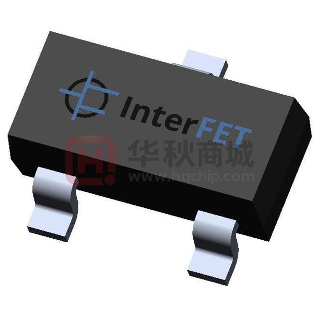
InterFET
Product
Folder
Technical
Support
J176-7
Order
Now
J176, J177 P-Channel JFET
Features
•
•
•
•
•
InterFET P0099F Geometry
Low Noise: 8 nV/√Hz Typical
Low Rds(on): 150 Ohms Typical
RoHS Compliant
SMT, TH, and Bare Die Package options.
SOT23 Top View
Source
1
3 Gate
Drain
Applications
2
• Choppers
• Commutators
• Analog Switches
TO-92 Bottom View
Description
Drain 3
The 30V InterFET J176 and J177 JFET’s are
targeted for high gain low noise switching,
commutator, and chopper applications.
Gate
2
Source
1
Product Summary
BVGSS
IDSS
VGS(off)
Parameters
Gate to Source Breakdown Voltage
Drain to Source Saturation Current
Gate to Source Cutoff Voltage
J176 Min
30
-2
1
J177 Min
30
-1.5
0.8
Unit
V
mA
V
Ordering Information Custom Part and Binning Options Available
Part Number
J176; J177
SMPJ176; SMPJ177
SMPJ176TR; SMPJ177TR
J176COT; J177COT
J176CFT; J177CFT
Description
Through-Hole
Surface Mount
7“ Tape and Reel: Max 3,000 Pieces
13” Tape and Reel: Max 9,000 Pieces
Chip Orientated Tray (COT Waffle Pack)
Chip Face-up Tray (CFT Waffle Pack)
Case
TO-92
SOT23
SOT23
COT
CFT
Packaging
Bulk
Bulk
Minimum 1,000 Pieces
Tape and Reel
400/Waffle Pack
400/Waffle Pack
Disclaimer: It is the Buyers responsibility for designing, validating and testing the end application under all field use cases and
extreme use conditions. Guaranteeing the application meets required standards, regulatory compliance, and all safety and
security requirements is the responsibility of the Buyer. These resources are subject to change without notice.
IF35089.R00
�InterFET
Product
Folder
Technical
Support
J176-7
Order
Now
Electrical Characteristics
Maximum Ratings (@ TA = 25°C, Unless otherwise specified)
VRGS
IFG
PD
P
TJ
TSTG
Parameters
Reverse Gate Source and Gate Drain Voltage
Continuous Forward Gate Current
Continuous Device Power Dissipation
Power Derating
Operating Junction Temperature
Storage Temperature
Value
30
50
360
3.27
-55 to 125
-65 to 200
Unit
V
mA
mW
mW/°C
°C
°C
Static Characteristics (@ TA = 25°C, Unless otherwise specified)
J176
V(BR)GSS
IGSS
VGS(OFF)
IDSS
ID(OFF)
Parameters
Gate to Source
Breakdown Voltage
Gate to Source
Reverse Current
Gate to Source
Cutoff Voltage
Drain to Source
Saturation Current
Drain Cutoff Current
Conditions
Min
VDS = 0V, IG = 1μA
30
J177
Max
Min
Max
30
VGS = 20V, VDS = 0V
Unit
V
1
1
nA
VDS = -15V, ID = -10nA
1
4
0.8
2.25
V
VGS = 0V, VDS = -15V
(Pulsed)
-2
-35
-1.5
-20
mA
-1
nA
Max
Unit
300
Ω
VDS = -15V, VGS = 10V
-1
Dynamic Characteristics (@ TA = 25°C, Unless otherwise specified)
J176
RDS(ON)
Cgd
Parameters
Drain to Source
ON Resistance
Drain Gate
Capacitance
Cgs
Input Capacitance
Cgd + Cgs
Drain + Source Gate
Capacitance
td(ON)
Turn ON Delay Time
tr
Rise Time
td(OFF)
Turn OFF Delay Time
tf
Fall Time
J176-7
Document Number: IF35089.R00
Conditions
VDS
很抱歉,暂时无法提供与“SMPJ177”相匹配的价格&库存,您可以联系我们找货
免费人工找货