5962-0625501QHC
®
Data Sheet
May 2, 2007
350MHz Fixed Gain Amplifiers with Enable
Features
The 5962-0625501QHC is a fully DSCC SMD compliant part
and the SMD data sheet is available on the DSCC website
(http://www.dscc.dla.mil/programs/specfind/default.asp).
The 5962-0625501QHC is electrically equivalent to the
EL5106. Reference equivalent “EL” data sheet for additional
information. The 5962-0625501QHC is a fixed gain amplifier
with a bandwidth of 350MHz. This amplifier is ideal for
today’s high speed video and monitor applications. It
features internal gain setting resistors and can be configured
in a gain of +1, -1 or +2.
• Gain selectable (+1, -1, +2)
With a supply current of just 1.5mA and the ability to run
from a single supply voltage from 5V to 12V, these amplifiers
are also ideal for handheld, portable or battery powered
equipment.
• Handheld, portable devices
The 5962-0625501QHC has an enable and disable function
to reduce the supply current to 25µA typical. Allowing the CE
pin to float or applying a low logic level will enable the
amplifier.
• RGB amplifiers
• 350MHz -3dB BW (AV = 2)
• 1.5mA supply current per amplifier
• Fast enable/disable
• Single and dual supply operation, from 5V to 12V
Applications
• Battery powered equipment
• Video amplifiers
• Cable drivers
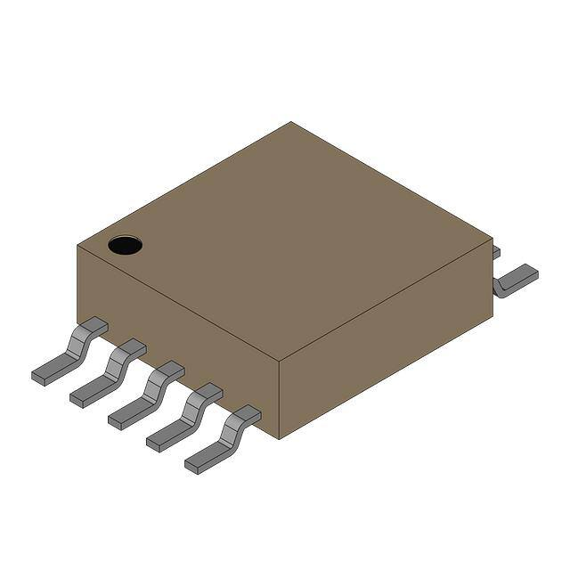
Pinout
5962-0625501QHC
(10 LD FLAT PACK)
TOP VIEW
Ordering Information
PART NUMBER
5962-0625501QHC
PART
MARKING
06255 01QHC
PACKAGE
PKG.
DWG. #
10 Ld Flat Pack K10.A
1
2
3
4
5
1
FN6490.0
NC
NC
IN-
NC
IN+
CE
VS-
VS+
NC
OUT
10
9
8
7
6
CAUTION: These devices are sensitive to electrostatic discharge; follow proper IC Handling Procedures.
1-888-INTERSIL or 1-888-468-3774 | Intersil (and design) is a registered trademark of Intersil Americas Inc.
Copyright © Intersil Americas Inc. 2007. All Rights Reserved.
All other trademarks mentioned are the property of their respective owners.
�5962-0625501QHC
Absolute Maximum Ratings (TA = +25°C)
Thermal Information
Supply Voltage between VS+ and VS- . . . . . . . . . . . . . . . . . . . 13.2V
Pin Voltages . . . . . . . . . . . . . . . . . . . . . . . . . VS- -0.5V to VS+ +0.5V
Maximum Continuous Output Current . . . . . . . . . . . . . . . . . . . 20mA
Thermal Resistance (Typical)
θJA (°C/W)
θJC (°C/W)
Flat Pack Package (Notes 1, 2) . . . . . .
165
60
Storage Temperature . . . . . . . . . . . . . . . . . . . . . . . .-65°C to +150°C
Ambient Operating Temperature . . . . . . . . . . . . . . .-55°C to +125°C
Operating Junction Temperature . . . . . . . . . . . . . . . . . . . . . . +150°C
Power Dissipation . . . . . . . . . . . . . . . . . . . . . . . . . . . . . . . . 21.8mW
CAUTION: Stresses above those listed in “Absolute Maximum Ratings” may cause permanent damage to the device. This is a stress only rating and operation of the
device at these or any other conditions above those indicated in the operational sections of this specification is not implied.
NOTES:
1. θJA is measured with the component mounted on a low effective thermal conductivity test board in free air. See Tech Brief TB379 for details.
2. For θJC, the “case temp” location is the center of the exposed metal pad on the package underside.
IMPORTANT NOTE: All parameters having Min/Max specifications are guaranteed. Typical values are for information purposes only. Unless otherwise noted, all tests
are at the specified temperature and are pulsed tests, therefore: TJ = TC = TA
Electrical Specifications
PARAMETER
VS+ = +5V, VS- = -5V, RL = 150Ω, TA = +25°C unless otherwise specified.
DESCRIPTION
CONDITIONS
MIN
TYP
MAX
UNIT
AC PERFORMANCE
BW
-3dB Bandwidth
AV = +1
250
MHz
AV = -1
380
MHz
AV = +2
350
MHz
20
MHz
4500
V/µs
16
ns
2.8
nV/√Hz
6
pA/√Hz
BW1
0.1dB Bandwidth
SR
Slew Rate
VO = -2.5V to +2.5V, AV = +2
tS
0.1% Settling Time
VOUT = -2.5V to +2.5V, AV = 2
eN
Input Voltage Noise
iN+
IN+ Input Current Noise
dG
Differential Gain Error (Note 3)
AV = +2
0.02
%
dP
Differential Phase Error (Note 3)
AV = +2
0.04
°
325
Ω
2
MΩ
1
pF
DC PERFORMANCE
RF, RG
Internal RF and RG
INPUT CHARACTERISTICS
RIN
Input Resistance
CIN
Input Capacitance
at IN+
ENABLE
tEN
Enable Time
280
ns
tDIS
Disable Time
400
ns
NOTE:
3. Standard NTSC test, AC signal amplitude = 286mVP-P, f = 3.58MHz
2
�5962-0625501QHC
Pin Descriptions
5962-0625501QHCIS
(10 LD FLAT PACK)
PIN
NAME
1, 5, 9, 10
NC
Not connected
2
IN-
Inverting input
FUNCTION
EQUIVALENT CIRCUIT
RG
IN+
IN-
RF
CIRCUIT 1
3
IN+
Non-inverting input
4
VS-
Negative supply
6
OUT
Output
(Reference Circuit 1)
OUT
RF
CIRCUIT 2
7
VS+
Positive supply
8
CE
Chip enable
VS+
CE
VSCIRCUIT 3
All Intersil U.S. products are manufactured, assembled and tested utilizing ISO9000 quality systems.
Intersil Corporation’s quality certifications can be viewed at www.intersil.com/design/quality
Intersil products are sold by description only. Intersil Corporation reserves the right to make changes in circuit design, software and/or specifications at any time without
notice. Accordingly, the reader is cautioned to verify that data sheets are current before placing orders. Information furnished by Intersil is believed to be accurate and
reliable. However, no responsibility is assumed by Intersil or its subsidiaries for its use; nor for any infringements of patents or other rights of third parties which may result
from its use. No license is granted by implication or otherwise under any patent or patent rights of Intersil or its subsidiaries.
For information regarding Intersil Corporation and its products, see www.intersil.com
3
�5962-0625501QHC
Ceramic Metal Seal Flatpack Packages (Flatpack)
K10.A MIL-STD-1835 CDFP3-F10 (F-4A, CONFIGURATION B)
10 LEAD CERAMIC METAL SEAL FLATPACK PACKAGE
e
A
INCHES
A
-A-
D
-BPIN NO. 1
ID AREA
b
E1
0.004 M
H A-B S
Q
D S
S1
0.036 M
H A-B S
D S
C
E
-D-
A
-C-
-HL
E2
E3
SEATING AND
BASE PLANE
c1
L
E3
(c)
b1
M
M
(b)
SECTION A-A
NOTES:
1. Index area: A notch or a pin one identification mark shall be located adjacent to pin one and shall be located within the shaded
area shown. The manufacturer’s identification shall not be used
as a pin one identification mark. Alternately, a tab (dimension k)
may be used to identify pin one.
2. If a pin one identification mark is used in addition to a tab, the limits of dimension k do not apply.
3. This dimension allows for off-center lid, meniscus, and glass
overrun.
4. Dimensions b1 and c1 apply to lead base metal only. Dimension
M applies to lead plating and finish thickness. The maximum limits of lead dimensions b and c or M shall be measured at the centroid of the finished lead surfaces, when solder dip or tin plate
lead finish is applied.
5. N is the maximum number of terminal positions.
6. Measure dimension S1 at all four corners.
7. For bottom-brazed lead packages, no organic or polymeric materials shall be molded to the bottom of the package to cover the
leads.
8. Dimension Q shall be measured at the point of exit (beyond the
meniscus) of the lead from the body. Dimension Q minimum
shall be reduced by 0.0015 inch (0.038mm) maximum when solder dip lead finish is applied.
9. Dimensioning and tolerancing per ANSI Y14.5M - 1982.
10. Controlling dimension: INCH.
4
MIN
MILLIMETERS
MAX
MIN
MAX
NOTES
A
0.045
0.115
1.14
2.92
-
b
0.015
0.022
0.38
0.56
-
b1
0.015
0.019
0.38
0.48
-
c
0.004
0.009
0.10
0.23
-
c1
0.004
0.006
0.10
0.15
-
D
-
0.290
-
7.37
3
E
0.240
0.260
6.10
6.60
-
E1
-
0.280
-
7.11
3
E2
0.125
-
3.18
-
-
E3
0.030
-
0.76
-
7
2
e
LEAD FINISH
BASE
METAL
SYMBOL
0.050 BSC
1.27 BSC
-
k
0.008
0.015
0.20
0.38
L
0.250
0.370
6.35
9.40
-
Q
0.026
0.045
0.66
1.14
8
S1
0.005
-
0.13
-
6
M
-
0.0015
-
0.04
-
N
10
10
Rev. 0 3/07
�
很抱歉,暂时无法提供与“5962-0625501QHC”相匹配的价格&库存,您可以联系我们找货
免费人工找货