DG201A, DG202
T
UC T
R OD R OD U C
P
E
P
,
T
)
E
E
P
DI
OL
UT
OBS UBSTIT DG441(P42
S
4
,
)
E
, DG Sheet
R DIP C)Data
SIBL
POS 0201(CE1HS(SOI
HI1- I9P020
H
itle
G20
,
202
bt
uad
ST,
OS
a-
May 2001
File Number
3117.3
Quad SPST, CMOS Analog Switches
Features
The DG201A and DG202 quad SPST analog switches are
designed using Intersil’s 44V CMOS process. These
bidirectional switches are latch-proof and feature breakbefore-make switching. Designed to block signals up to
30V P-P in the OFF state, the DG201A and DG202 offer the
advantages of low ON resistance (≤175Ω), wide input signal
range (±15V) and provide both TTL and CMOS compatibility.
• Input Signal Range. . . . . . . . . . . . . . . . . . . . . . . . . . ±15V
• Low rDS(ON) (Max). . . . . . . . . . . . . . . . . . . . . . . . . . 175Ω
• TTL, CMOS Compatible
• Latch-Up Proof
• True Second Source
The DG201A and DG202 are specification and pinout
compatible with the industry standard devices.
• Maximum Supply Ratings . . . . . . . . . . . . . . . . . . . . . 44V
Part Number Information
Functional Block Diagrams
TEMP.
RANGE ( oC)
PART NUMBER
PACKAGE
• Logic Inputs Accept Negative Voltages
DG201A
PKG.
NO.
S1
itch
utho
)
eyrds
ter-
DG201AAK
-55 to 125
16 Ld CERDIP
F16.3
DG201ABK
-25 to 85
16 Ld CERDIP
F16.3
DG201ACJ
0 to 70
16 Ld PDIP
E16.3
DG201ACY
0 to 70
16 Ld SOIC
M16.3
16 Ld CERDIP
F16.3
16 Ld PDIP
E16.3
IN1
D1
S2
DG202AK
-55 to 125
DG202CJ
0 to 70
IN2
D2
S3
IN3
D3
S4
rpoion,
inctor,
itch
OS
PST,
DT,
ST,
DT,
eo,
ET,
alog
itch,
anl)
re-
IN4
Pinout
D4
DG201A, DG202
(CERDIP, PDIP, SOIC)
TOP VIEW
IN1
1
DG202
S1
16 IN 2
D1
2
15 D2
S1
3
14 S2
13 V+ (SUBSTRATE)
V- 4
GND
5
12 NC
S4
6
11 S3
D4
7
10 D3
IN4
8
IN1
D1
S2
IN2
D2
S3
IN3
D3
9 IN 3
S4
IN4
D4
SWITCHES SHOWN FOR LOGIC “1” INPUT
TRUTH TABLE
LOGIC
DG201A
DG202
0
ON
OFF
1
OFF
ON
Logic “0” ≤0.8V, Logic “1” ≥ 2.4V
1
CAUTION: These devices are sensitive to electrostatic discharge; follow proper IC Handling Procedures.
1-888-INTERSIL or 321-724-7143 | Intersil and Design is a trademark of Intersil Americas Inc. | Copyright © Intersil Americas Inc. 2001
�DG201A, DG202
Absolute Maximum Ratings
Thermal Information
V+ to V- . . . . . . . . . . . . . . . . . . . . . . . . . . . . . . . . . . . . . . . . . . . 44V
V- to Ground. . . . . . . . . . . . . . . . . . . . . . . . . . . . . . . . . . . . . . . . -25V
VIN to Ground (Note 1) . . . . . . . . . . . . . . . . . . . (V-) -2V to (V+) +2V
VS or VD to V+ (Note 1) . . . . . . . . . . . . . . . . . . . . . . . . +2 to (V-) -2V
VS or VD to V- (Note 1) . . . . . . . . . . . . . . . . . . . . . . . -2 to (V+) +2V
Current, any Terminal Except S or D . . . . . . . . . . . . . . . . . . . . 30mA
Continuous Current, S or D . . . . . . . . . . . . . . . . . . . . . . . . . . . 20mA
Peak Current, S or D (Pulsed 1ms, 10% Duty Cycle Max) . . . . . 70mA
Thermal Resistance (Typical, Note 2)
Operating Conditions
θJA ( oC/W)
θJC (oC/W)
CERDIP Package. . . . . . . . . . . . . . . . .
75
20
PDIP Package . . . . . . . . . . . . . . . . . . .
100
N/A
SOIC Package . . . . . . . . . . . . . . . . . . .
100
N/A
Maximum Junction Temperature
Ceramic Package . . . . . . . . . . . . . . . . . . . . . . . . . . . . . . . . 175oC
Plastic Package . . . . . . . . . . . . . . . . . . . . . . . . . . . . . . . . . 150oC
Maximum Storage Temperature Range . . . . . . . . . . -65oC to 150oC
Maximum Lead Temperature (Soldering 10s) . . . . . . . . . . . . 300oC
(SOIC - Lead Tips Only)
Temperature Range
“A” Suffix. . . . . . . . . . . . . . . . . . . . . . . . . . . . . . . . -55oC to 125oC
“B” Suffix. . . . . . . . . . . . . . . . . . . . . . . . . . . . . . . . . -25oC to 85oC
“C” Suffix . . . . . . . . . . . . . . . . . . . . . . . . . . . . . . . . . . 0oC to 70oC
CAUTION: Stresses above those listed in “Absolute Maximum Ratings” may cause permanent damage to the device. This is a stress only rating and operation of the
device at these or any other conditions above those indicated in the operational sections of this specification is not implied.
NOTES:
1. Signals on VS , VD , or VIN exceeding V+ or V- will be clamped by internal diodes. Limit forward diode current to maximum current ratings.
2. θJA is measured with the component mounted on an evaluation PC board in free air.
V+ = 15V, V- = -15V, GND = 0V, TA = 25oC
Electrical Specifications
“A” SUFFIX
PARAMETER
TEST CONDITIONS
“B” AND “C” SUFFIX
MIN
(NOTE 3)
TYP
MAX
MIN
(NOTE 3)
TYP
MAX
UNITS
DYNAMIC CHARACTERISTICS
Turn-ON Time, tON
See Figure 1
-
480
600
-
480
-
ns
Turn-OFF Time, tOFF
See Figure 1
-
370
450
-
370
-
ns
Charge Injection, Q
C L = 1nF, RS = 0, VS = 0V
-
20
-
-
20
-
pC
OFF Isolation, OIRR
VIN = 5V, RL = 75Ω, VS = 2.0V,
f = 100kHz
-
70
-
-
70
-
dB
-
-90
-
-
-90
-
dB
-
5.0
-
-
5.0
-
pF
Drain OFF Capacitance, CD(OFF)
-
5.0
-
-
5.0
-
pF
Channel ON Capacitance,
C D(ON) + CS(ON)
-
16
-
-
16
-
pF
VIN = 2.4V
-1.0
-0.0004
-
-1.0
-0.0004
-
µA
VIN = 15V
-
0.003
1.0
-
0.003
1.0
µA
VIN = 0V
-1.0
-0.0004
-
-1.0
-0.0004
-
µA
-15
-
15
-15
-
15
V
-
115
175
-
115
200
Ω
VS = 14V, VD = -14V
-
0.01
1.0
-
0.01
5.0
nA
VS = -14V, VD = 14V
-1.0
-0.02
-
-5.0
-0.02
-
nA
VS = -14V, VD = 14V
-
0.01
1.0
-
0.01
5.0
nA
V S = 14V, VD = -14V
-1.0
-0.02
-
-5.0
-0.02
-
nA
Crosstalk (Channel to Channel), CCRR
Source OFF Capacitance, CS(OFF)
f = 140kHz, VIN = 5V, VS = VD = 0V
DIGITAL INPUT CHARACTERISTICS
Input Current with Voltage High, IIH
Input Current with Voltage Low, IIL
ANALOG SWITCH CHARACTERISTICS
Analog Signal Range, VANALOG
Drain-Source ON Resistance, r DS(ON)
VD = ±10V, VIN = 0.8V (DG201A)
IS = 1mA, VIN = 2.4V (DG202)
Source OFF Leakage Current, IS(OFF)
VIN = 2.4V
(DG201A)
VIN = 0.8V
(DG202)
Drain OFF Leakage Current, ID(OFF)
2
�DG201A, DG202
V+ = 15V, V- = -15V, GND = 0V, TA = 25oC (Continued)
Electrical Specifications
“A” SUFFIX
PARAMETER
MIN
(NOTE 3)
TYP
MAX
MIN
(NOTE 3)
TYP
MAX
UNITS
VD = VS = 14V
-
0.1
1.0
-
0.1
5.0
µA
VD = VS = -14V
-1.0
-0.15
-
-5.0
-0.15
-
µA
-
0.9
2
-
0.9
2
mA
-1
-0.3
-
-1
-0.3
-
mA
TEST CONDITIONS
Drain ON Leakage Current, ID(ON)
(Note 5)
VIN = 0.8V
(DG201A)
VIN = 2.4V
(DG202)
“B” AND “C” SUFFIX
POWER SUPPLY CHARACTERISTICS
Positive Supply Current, I+
All Channels ON or OFF
Negative Supply Current, I-
Electrical Specifications
V+ = 15V, V- = -15V, GND = 0V, TA Over Operating Temperature Range
“A” SUFFIX
MIN
(NOTE 3)
TYP
MAX
UNITS
VIN = 2.4V
-10
-
-
µA
VIN = 15V
-
-
10
µA
VIN = 0V
-10
-
-
µA
-15
-
15
V
PARAMETER
TEST CONDITIONS
DIGITAL INPUT CHARACTERISTICS
Input Current with Voltage High, IIH
Input Current with Voltage Low, IIL
ANALOG SWITCH CHARACTERISTICS
Analog Signal Range, VANALOG
Drain-Source ON Resistance, r DS(ON)
VD = ±10V, VIN = 0.8V (DG201A)
IS = 1mA, VIN = 2.4V (DG202)
-
-
250
Ω
Source OFF Leakage Current, IS(OFF)
VIN = 2.4V (DG201A)
VIN = 0.8V (DG202)
VS = 14V, VD = -14V
-
-
100
nA
VS = -14V, VD = 14V
-100
-
-
nA
VS = -14V, VD = 14V
-
-
100
nA
VS = 14V, VD = -14V
-100
-
-
nA
VD = VS = 14V
-
-
200
µA
VD = VS = -14V
-200
-
-
µA
Drain OFF Leakage Current, ID(OFF)
Drain ON Leakage Current, ID(ON) (Note 5)
VIN = 0.8V (DG201A)
VIN = 2.4V (DG202)
NOTES:
3. Typical values are for design aid only, not guaranteed and not subject to production testing.
4. The algebraic convention whereby the most negative value is a minimum, and the most positive is a maximum, is used in this data sheet.
5. ID(ON) is leakage from driver into ON switch.
3
�DG201A, DG202
Test Circuits and Waveforms
LOGIC † 3V
INPUT
SWITCH
INPUT
RL + rDS(ON)
15V
V+
50%
tr < 20ns
tf < 20ns
RL
VO = VS
LOGIC “0” = SWITCH ON
SWITCH
INPUT
S1
SWITCH
OUTPUT
VO
D1
VS = 2V
VS
90%
90%
SWITCH
OUTPUT
tON
LOGIC
INPUT
RL
1kΩ
IN1
tOFF
(REPEAT TEST FOR
IN2 , IN 3 AND IN 4)
GND
V-15V
† Logic shown for DG201A, invert for DG202.
CL
35pF
FIGURE 1. tON AND tOFF SWITCHING TEST CIRCUIT AND MEASUREMENT POINTS
∆VO
RS
SX
DX
VO
INX
VS
SWITCH
OUTPUT
CL = 1nF
INX
ON
ON
OFF
NOTES:
6. ∆VO = Measured voltage error due to charge injection.
7. The error in coulombs is Q = CL x ∆VO .
FIGURE 2. CHARGE INJECTION TEST CIRCUIT AND MEASUREMENT POINTS
+15V
+15V
C
C
V+
VS
SIGNAL
GENERATOR
SIGNAL
GENERATOR
VS
3
V+
VS1
50Ω
VD1
VS
INX
VIN
ANALYZER
CHAN A
ANALYZER
CHAN A
VD
CHAN B
GND
0V,
2.4V
V-
V
S
O IRR = 20 Log ------VD
FIGURE 3. OFF ISOLATION TEST CIRCUIT
4
NC
V-
RL
C
-15V
-15V
C = 0.001µF|| 0.1µF
Chip Capacitors
VS2
GND
C
0V, 2.4V
IN2
VD2
CHAN B
RL
IN1
C = 0.001µF || 0.1µF
Chip Capacitors
V
S1
CCRR = 20 Log ----------VD 2
FIGURE 4. CHANNEL TO CHANNEL CROSSTALK TEST
CIRCUIT
�DG201A, DG202
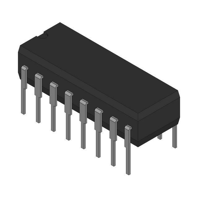
Dual-In-Line Plastic Packages (PDIP)
N
E16.3 (JEDEC MS-001-BB ISSUE D)
16 LEAD DUAL-IN-LINE PLASTIC PACKAGE
E1
INDEX
AREA
1 2 3
N/2
INCHES
-B-
SYMBOL
-AD
E
BASE
PLANE
-C-
A2
SEATING
PLANE
A
L
D1
e
B1
D1
eA
A1
eC
B
C
L
0.010 (0.25) M C A B S
MAX
MIN
MAX
NOTES
A
-
A1
0.015
0.210
-
5.33
4
-
0.39
-
4
A2
0.115
0.195
2.93
4.95
-
B
0.014
0.022
0.356
0.558
-
B1
0.045
0.070
1.15
1.77
8, 10
C
0.008
0.014
0.204
0.355
-
C
eB
NOTES:
1. Controlling Dimensions: INCH. In case of conflict between English and
Metric dimensions, the inch dimensions control.
2. Dimensioning and tolerancing per ANSI Y14.5M-1982.
3. Symbols are defined in the “MO Series Symbol List” in Section 2.2 of
Publication No. 95.
4. Dimensions A, A1 and L are measured with the package seated in JEDEC seating plane gauge GS-3.
5. D, D1, and E1 dimensions do not include mold flash or protrusions.
Mold flash or protrusions shall not exceed 0.010 inch (0.25mm).
6. E and eA are measured with the leads constrained to be perpendicular to datum -C- .
7. eB and eC are measured at the lead tips with the leads unconstrained.
eC must be zero or greater.
8. B1 maximum dimensions do not include dambar protrusions. Dambar
protrusions shall not exceed 0.010 inch (0.25mm).
9. N is the maximum number of terminal positions.
10. Corner leads (1, N, N/2 and N/2 + 1) for E8.3, E16.3, E18.3, E28.3,
E42.6 will have a B1 dimension of 0.030 - 0.045 inch (0.76 - 1.14mm).
5
MILLIMETERS
MIN
D
0.735
0.775
18.66
19.68
5
D1
0.005
-
0.13
-
5
E
0.300
0.325
7.62
8.25
6
E1
0.240
0.280
6.10
7.11
5
e
0.100 BSC
2.54 BSC
-
eA
0.300 BSC
7.62 BSC
6
eB
-
0.430
-
L
0.115
0.150
2.93
N
16
16
10.92
7
3.81
4
9
Rev. 0 12/93
�DG201A, DG202
Ceramic Dual-In-Line Frit Seal Packages (CERDIP)
F16.3 MIL-STD-1835 GDIP1-T16 (D-2, CONFIGURATION A)
16 LEAD CERAMIC DUAL-IN-LINE FRIT SEAL PACKAGE
LEAD FINISH
c1
-D-
-A-
BASE
METAL
E
M
-Bbbb S
C A-B S
-C-
S1
0.200
-
5.08
-
0.026
0.36
0.66
2
b1
0.014
0.023
0.36
0.58
3
b2
0.045
0.065
1.14
1.65
-
eA
ccc M C A - B S
e
eA/2
c
aaa M C A - B S D S
D S
NOTES
-
b2
b
MAX
0.014
α
A A
MIN
b
A
L
MAX
A
Q
SEATING
PLANE
MILLIMETERS
MIN
M
(b)
D
BASE
PLANE
SYMBOL
b1
SECTION A-A
D S
INCHES
(c)
NOTES:
1. Index area: A notch or a pin one identification mark shall be located adjacent to pin one and shall be located within the shaded
area shown. The manufacturer’s identification shall not be used
as a pin one identification mark.
b3
0.023
0.045
0.58
1.14
4
c
0.008
0.018
0.20
0.46
2
c1
0.008
0.015
0.20
0.38
3
D
-
0.840
-
21.34
5
E
0.220
0.310
5.59
7.87
5
e
0.100 BSC
2.54 BSC
-
eA
0.300 BSC
7.62 BSC
-
eA/2
0.150 BSC
3.81 BSC
-
L
0.125
0.200
3.18
5.08
-
Q
0.015
0.060
0.38
1.52
6
S1
0.005
-
0.13
-
7
105o
90o
105o
-
2. The maximum limits of lead dimensions b and c or M shall be
measured at the centroid of the finished lead surfaces, when
solder dip or tin plate lead finish is applied.
α
90o
aaa
-
0.015
-
0.38
-
3. Dimensions b1 and c1 apply to lead base metal only. Dimension
M applies to lead plating and finish thickness.
bbb
-
0.030
-
0.76
-
ccc
-
0.010
-
0.25
-
M
-
0.0015
-
0.038
2, 3
4. Corner leads (1, N, N/2, and N/2+1) may be configured with a
partial lead paddle. For this configuration dimension b3 replaces
dimension b2.
5. This dimension allows for off-center lid, meniscus, and glass
overrun.
6. Dimension Q shall be measured from the seating plane to the
base plane.
7. Measure dimension S1 at all four corners.
8. N is the maximum number of terminal positions.
9. Dimensioning and tolerancing per ANSI Y14.5M - 1982.
10. Controlling dimension: INCH.
6
N
16
16
8
Rev. 0 4/94
�DG201A, DG202
Small Outline Plastic Packages (SOIC)
N
M16.3 (JEDEC MS-013-AA ISSUE C)
INDEX
AREA
0.25(0.010) M
H
B M
16 LEAD WIDE BODY SMALL OUTLINE PLASTIC PACKAGE
E
INCHES
-B-
1
2
3
L
SEATING PLANE
-A-
h x 45o
A
D
-C-
e
µα
B
0.25(0.010) M
C
0.10(0.004)
C A M
MIN
MAX
MIN
MAX
NOTES
A
0.0926
0.1043
2.35
2.65
-
A1
0.0040
0.0118
0.10
0.30
-
B
0.013
0.0200
0.33
0.51
9
C
0.0091
0.0125
0.23
0.32
-
D
0.3977
0.4133
10.10
10.50
3
E
0.2914
0.2992
7.40
7.60
4
e
A1
B S
0.050 BSC
1. Symbols are defined in the “MO Series Symbol List” in Section 2.2 of
Publication Number 95.
1.27 BSC
-
H
0.394
0.419
10.00
10.65
-
h
0.010
0.029
0.25
0.75
5
L
0.016
0.050
0.40
1.27
6
8o
0o
N
NOTES:
MILLIMETERS
SYMBOL
α
16
0o
16
7
8o
Rev. 0 12/93
2. Dimensioning and tolerancing per ANSI Y14.5M-1982.
3. Dimension “D” does not include mold flash, protrusions or gate burrs.
Mold flash, protrusion and gate burrs shall not exceed 0.15mm (0.006
inch) per side.
4. Dimension “E” does not include interlead flash or protrusions. Interlead
flash and protrusions shall not exceed 0.25mm (0.010 inch) per side.
5. The chamfer on the body is optional. If it is not present, a visual index
feature must be located within the crosshatched area.
6. “L” is the length of terminal for soldering to a substrate.
7. “N” is the number of terminal positions.
8. Terminal numbers are shown for reference only.
9. The lead width “B”, as measured 0.36mm (0.014 inch) or greater above
the seating plane, shall not exceed a maximum value of 0.61mm (0.024
inch)
10. Controlling dimension: MILLIMETER. Converted inch dimensions are
not necessarily exact.
All Intersil products are manufactured, assembled and tested utilizing ISO9000 quality systems.
Intersil Corporation’s quality certifications can be viewed at website www.intersil.com/design/quality/iso.asp
Intersil products are sold by description only. Intersil Corporation reserves the right to make changes in circuit design and/or specifications at any time without notice.
Accordingly, the reader is cautioned to verify that data sheets are current before placing orders. Information furnished by Intersil is believed to be accurate and reliable. However, no responsibility is assumed by Intersil or its subsidiaries for its use; nor for any infringements of patents or other rights of third parties which may result from its use.
No license is granted by implication or otherwise under any patent or patent rights of Intersil or its subsidiaries.
For information regarding Intersil Corporation and its products, see web site www.intersil.com
Sales Office Headquarters
EUROPE
Intersil SA
Mercure Center
100, Rue de la Fusee
1130 Brussels, Belgium
TEL: (32) 2.724.2111
FAX: (32) 2.724.22.05
NORTH AMERICA
Intersil Corporation
2401 Palm Bay Rd.
Palm Bay, FL 32905
TEL: (321) 724-7000
FAX: (321) 724-7240
7
ASIA
Intersil Ltd.
8F-2, 96, Sec. 1, Chien-kuo North,
Taipei, Taiwan 104
Republic of China
TEL: 886-2-2515-8508
FAX: 886-2-2515-8369
�