HA-5033
Data Sheet
September 1998
File Number
2924.4
250MHz Video Buffer
Features
The HA-5033 is a unity gain monolithic IC designed for any
application requiring a fast, wideband buffer. Featuring a
bandwidth of 250MHz and outstanding differential phase/
gain characteristics, this high performance voltage follower is
an excellent choice for video circuit design. Other features,
which include a minimum slew rate of 1000V/µs and high
output drive capability, make the HA-5033 applicable for line
driver and high speed data conversion circuits.
• Differential Phase Error . . . . . . . . . . . . . . . 0.02 Degrees
• Differential Gain Error. . . . . . . . . . . . . . . . . . . . . . . 0.03%
• High Slew Rate. . . . . . . . . . . . . . . . . . . . . . . . . . 1100V/µs
• Wide Bandwidth (Small Signal) . . . . . . . . . . . . . . 250MHz
• Wide Power Bandwidth . . . . . . . . . . . . . . DC to 17.5MHz
• Fast Rise Time . . . . . . . . . . . . . . . . . . . . . . . . . . . . . . 3ns
• High Output Drive. . . . . . . . . . . . . . ±10V With 100Ω Load
The high performance of this product is a result of the Intersil
Dielectric Isolation process. A major feature of this process
is that it produces both PNP and NPN high frequency
transistors which makes wide bandwidth designs, such as
the HA-5033, practical. Alternative process methods
typically produce a lower AC performance.
• Wide Power Supply Range. . . . . . . . . . . . . . ±5V to ±16V
• Replace Costly Hybrids
Applications
• Video Buffer
Ordering Information
PART NUMBER
(BRAND)
• High Frequency Buffer
TEMP.
RANGE (oC)
PKG.
NO.
PACKAGE
HA2-5033-2
-55 to 125
12 Pin Metal Can
T12.C
• High Speed Line Driver
HA2-5033-5
0 to 75
12 Pin Metal Can
T12.C
• Impedance Matching
HA3-5033-5
0 to 75
8 Ld PDIP
E8.3
• Current Boosters
HA4P5033-5
0 to 75
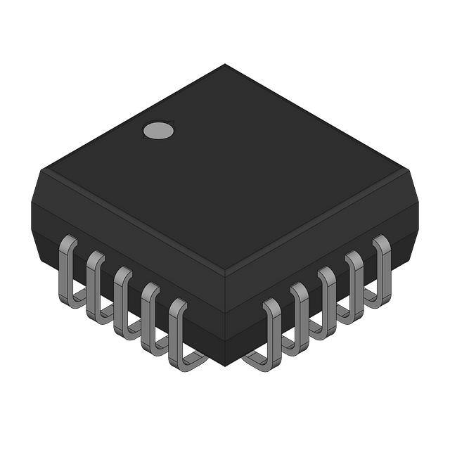
20 Ld PLCC
N20.35
• High Speed A/D Input Buffers
HA9P5033-5
(H50335)
0 to 60
(Note 3)
8 Ld PSOP
M8.15A
• Related Literature
- AN548, Designer’s Guide for HA-5033
• Isolation Buffer
Pinouts
NC
OUT
OUT
8
NC
V+ 1
HA-5033
(METAL CAN)
TOP VIEW
V+
HA-5033
(PLCC)
TOP VIEW
NC
HA-5033
(PDIP, PSOP)
TOP VIEW
3
2
1
20
19
V+
NC
CASE
3
6
4
5
NC
SUBSTRATE
V-
NC 4
18 NC
NC 5
17 NC
NC 6
16 NC
NC 7
15 SUBSTRATE
14 NC
1
9
10
11
12
13
V-
NC
NC 8
NC
IN
7
IN
NC
2
NC
NC
OUT
12
11
1
NC
V-
10
2
9
3
4
NC
NC
8
NC
7
5
6
+IN
NC
NC
CAUTION: These devices are sensitive to electrostatic discharge; follow proper IC Handling Procedures.
1-888-INTERSIL or 321-724-7143 | Copyright © Intersil Corporation 1999
�HA-5033
Absolute Maximum Ratings
Thermal Information
Voltage Between V+ and V- Pins . . . . . . . . . . . . . . . . . . . . . . . . 40V
DC Input Voltage . . . . . . . . . . . . . . . . . . . . . . . . . . . . . . . . . V+ to VOutput Current (Peak) (50ms On/1 Second Off) . . . . . . . . . ±200mA
ESD Rating
Human Body Model (Per MIL-STD-883 Method 3015.7) . . . . 2000V
Thermal Resistance (Typical, Note 2)
θJA (oC/W) θJC (oC/W)
Metal Can Package . . . . . . . . . . . . . . .
65
34
PDIP Package . . . . . . . . . . . . . . . . . . .
96
N/A
PSOP Package (Note 4) . . . . . . . . . . .
129
N/A
PLCC Package. . . . . . . . . . . . . . . . . . .
80
N/A
Maximum Junction Temperature (Note 1) . . . . . . . . . . . . . . . . .175oC
Maximum Junction Temperature (Plastic Packages) . . . . . . .150oC
Maximum Storage Temperature Range . . . . . . . . . . -65oC to 150oC
Maximum Lead Temperature (Soldering 10s) . . . . . . . . . . . . 300oC
(PSOP and PLCC - Lead Tips Only)
Operating Conditions
Temperature Ranges
HA-5033-2 . . . . . . . . . . . . . . . . . . . . . . . . . . . . . . -55oC to 125oC
HA-5033-5 (Note 3) . . . . . . . . . . . . . . . . . . . . . . . . . 0oC to 75oC
HA9P5033-5 (Notes 1, 3) . . . . . . . . . . . . . . . . . . . . -40oC to 60oC
CAUTION: Stresses above those listed in “Absolute Maximum Ratings” may cause permanent damage to the device. This is a stress only rating and operation of the
device at these or any other conditions above those indicated in the operational sections of this specification is not implied.
NOTES:
1. Maximum power dissipation, including load conditions, must be designed to maintain the maximum junction temperature below 175oC for the metal
can package, and below 150oC for the plastic packages (See Figure 5.).
2. θJA is measured with the component mounted on an evaluation PC board in free air.
3. Maximum operating temperature in the PSOP package is limited to 60oC, for VSUPPLY = ±12V to prevent the junction temperature from exceeding 150oC. The maximum operating temperature may have to be derated further, depending on the output load condition. The operating temperature may be increased if the HA9P5033 is operated at lower VSUPPLY. For example, the quiescent operating temperature may be increased
to 75oC by operating at VSUPPLY ≤ ±9.7V. See Figure 5 for more information.
4. Direct attach of the PSOP copper slug to copper area on the PCB can reduce the θJA value to
很抱歉,暂时无法提供与“HA4P5033-5”相匹配的价格&库存,您可以联系我们找货
免费人工找货