HGTG30N60B3
Data Sheet January 2000 File Number 4444.2
60A, 600V, UFS Series N-Channel IGBT
The HGTG30N60B3 is a MOS gated high voltage switching device combining the best features of MOSFETs and bipolar transistors. This device has the high input impedance of a MOSFET and the low on-state conduction loss of a bipolar transistor. The much lower on-state voltage drop varies only moderately between 25oC and 150oC. The IGBT is ideal for many high voltage switching applications operating at moderate frequencies where low conduction losses are essential, such as: AC and DC motor controls, power supplies and drivers for solenoids, relays and contactors. Formerly Developmental Type TA49170.
Features
• 60A, 600V, TC = 25oC • 600V Switching SOA Capability • Typical Fall Time. . . . . . . . . . . . . . . . . 90ns at TJ = 150oC • Short Circuit Rating • Low Conduction Loss
Packaging
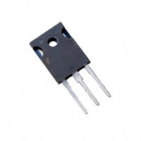
JEDEC STYLE TO-247
E C G
Ordering Information
PART NUMBER HGTG30N60B3 PACKAGE TO-247 BRAND G30N60B3
NOTE: When ordering, use the entire part number.
Symbol
C
G
E
INTERSIL CORPORATION IGBT PRODUCT IS COVERED BY ONE OR MORE OF THE FOLLOWING U.S. PATENTS 4,364,073 4,598,461 4,682,195 4,803,533 4,888,627 4,417,385 4,605,948 4,684,413 4,809,045 4,890,143 4,430,792 4,620,211 4,694,313 4,809,047 4,901,127 4,443,931 4,631,564 4,717,679 4,810,665 4,904,609 4,466,176 4,639,754 4,743,952 4,823,176 4,933,740 4,516,143 4,639,762 4,783,690 4,837,606 4,963,951 4,532,534 4,641,162 4,794,432 4,860,080 4,969,027 4,587,713 4,644,637 4,801,986 4,883,767
1
CAUTION: These devices are sensitive to electrostatic discharge; follow proper ESD Handling Procedures. 1-888-INTERSIL or 321-724-7143 | Copyright © Intersil Corporation 2000
�HGTG30N60B3
Absolute Maximum Ratings
TC = 25oC, Unless Otherwise Specified HGTG30N60B3 Collector to Emitter Voltage . . . . . . . . . . . . . . . . . . . . . . . . . . . . . . . . . . . . . . . . . . . . . .BVCES Collector Current Continuous At TC = 25oC . . . . . . . . . . . . . . . . . . . . . . . . . . . . . . . . . . . . . . . . . . . . . . . . . . . . . . . . . IC25 At TC = 110oC . . . . . . . . . . . . . . . . . . . . . . . . . . . . . . . . . . . . . . . . . . . . . . . . . . . . . . . IC110 Collector Current Pulsed (Note 1) . . . . . . . . . . . . . . . . . . . . . . . . . . . . . . . . . . . . . . . . . . . ICM Gate to Emitter Voltage Continuous. . . . . . . . . . . . . . . . . . . . . . . . . . . . . . . . . . . . . . . . . VGES Gate to Emitter Voltage Pulsed . . . . . . . . . . . . . . . . . . . . . . . . . . . . . . . . . . . . . . . . . . . VGEM Switching Safe Operating Area at TJ = 150oC (Figure 2) . . . . . . . . . . . . . . . . . . . . . . . SSOA Power Dissipation Total at TC = 25oC . . . . . . . . . . . . . . . . . . . . . . . . . . . . . . . . . . . . . . . . . PD Power Dissipation Derating TC > 25oC . . . . . . . . . . . . . . . . . . . . . . . . . . . . . . . . . . . . . . . . . . Reverse Voltage Avalanche Energy. . . . . . . . . . . . . . . . . . . . . . . . . . . . . . . . . . . . . . . . . EARV Operating and Storage Junction Temperature Range . . . . . . . . . . . . . . . . . . . . . . . . TJ, TSTG Maximum Lead Temperature for Soldering . . . . . . . . . . . . . . . . . . . . . . . . . . . . . . . . . . . . . TL Short Circuit Withstand Time (Note 2) at VGE = 12V. . . . . . . . . . . . . . . . . . . . . . . . . . . . . .tSC Short Circuit Withstand Time (Note 2) at VGE = 10V. . . . . . . . . . . . . . . . . . . . . . . . . . . . . .tSC 600 60 30 220 ±20 ±30 60A at 600V 208 1.67 100 -55 to 150 260 4 10 UNITS V A A A V V W W/oC mJ oC oC µs µs
CAUTION: Stresses above those listed in “Absolute Maximum Ratings” may cause permanent damage to the device. This is a stress only rating and operation of the device at these or any other conditions above those indicated in the operational sections of this specification is not implied.
NOTES: 1. Pulse width limited by maximum junction temperature. 2. VCE(PK) = 360V, TJ = 125oC, RG = 3Ω.
Electrical Specifications
PARAMETER
TC = 25oC, Unless Otherwise Specified SYMBOL BVCES BVECS ICES TEST CONDITIONS IC = 250µA, VGE = 0V IC = 10mA, VGE = 0V VCE = BVCES TC = 25oC TC = 150oC TC = 25oC TC = 150oC MIN 600 15 4.5 VCE (PK) = 480V VCE (PK) = 600V 200 60 TYP 28 1.45 1.7 5.0 MAX 250 3.0 1.9 2.1 6.0 ±250 UNITS V V µA mA V V V nA A A
Collector to Emitter Breakdown Voltage Emitter to Collector Breakdown Voltage Collector to Emitter Leakage Current
Collector to Emitter Saturation Voltage
VCE(SAT)
IC = IC110, VGE = 15V
Gate to Emitter Threshold Voltage Gate to Emitter Leakage Current Switching SOA
VGE(TH) IGES SSOA
IC = 250µA, VCE = VGE VGE = ±20V TJ = 150oC, RG = 3Ω, VGE = 15V L = 100µH,
Gate to Emitter Plateau Voltage On-State Gate Charge
VGEP QG(ON)
IC = IC110, VCE = 0.5 BVCES IC = IC110, VCE = 0.5 BVCES VGE = 15V VGE = 20V
-
7.2 170 230 36 25 137 58 500 550 680
190 250 800 900
V nC nC ns ns ns ns µJ µJ µJ
Current Turn-On Delay Time Current Rise Time Current Turn-Off Delay Time Current Fall Time Turn-On Energy (Note 4) Turn-On Energy (Note 4) Turn-Off Energy (Note 3)
td(ON)I trI td(OFF)I tfI EON1 EON2 EOFF
IGBT and Diode at TJ = 25oC ICE = IC110 VCE = 0.8 BVCES VGE = 15V RG= 3Ω L = 1mH Test Circuit (Figure 17)
2
�HGTG30N60B3
Electrical Specifications
PARAMETER Current Turn-On Delay Time Current Rise Time Current Turn-Off Delay Time Current Fall Time Turn-On Energy (Note 4) Turn-On Energy (Note 4) Turn-Off Energy (Note 3) Thermal Resistance Junction To Case NOTES: 3. Turn-Off Energy Loss (EOFF) is defined as the integral of the instantaneous power loss starting at the trailing edge of the input pulse and ending at the point where the collector current equals zero (ICE = 0A). All devices were tested per JEDEC Standard No. 24-1 Method for Measurement of Power Device Turn-Off Switching Loss. This test method produces the true total Turn-Off Energy Loss. 4. Values for two Turn-On loss conditions are shown for the convenience of the circuit designer. EON1 is the turn-on loss of the IGBT only. EON2 is the turn-on loss when a typical diode is used in the test circuit and the diode is at the same TJ as the IGBT. The diode type is specified in Figure 17. TC = 25oC, Unless Otherwise Specified (Continued) SYMBOL td(ON)I trI td(OFF)I tfI EON1 EON2 EOFF RθJC TEST CONDITIONS IGBT and Diode at TJ = 150oC ICE = IC110 VCE = 0.8 BVCES VGE = 15V RG= 3Ω L = 1mH Test Circuit (Figure 17) MIN TYP 32 24 275 90 500 1300 1600 MAX 320 150 1550 1900 0.6 UNITS ns ns ns ns µJ µJ µJ
oC/W
Typical Performance Curves
60 ICE , DC COLLECTOR CURRENT (A) 50 40 30 20 10 0
Unless Otherwise Specified
ICE, COLLECTOR TO EMITTER CURRENT (A) 225 200 175 150 125 100 75 50 25 0 0 100 200 300 400 500 600 700
VGE = 15V
TJ = 150oC, RG = 3Ω, VGE = 15V, L =100µH
25
50
75
100
125
150
TC , CASE TEMPERATURE (oC)
VCE, COLLECTOR TO EMITTER VOLTAGE (V)
FIGURE 1. DC COLLECTOR CURRENT vs CASE TEMPERATURE
fMAX, OPERATING FREQUENCY (kHz) TJ = 150oC, RG = 3Ω, L = 1mH, V CE = 480V
FIGURE 2. MINIMUM SWITCHING SAFE OPERATING AREA
tSC , SHORT CIRCUIT WITHSTAND TIME (µs)
100
VCE = 360V, RG = 3Ω, TJ = 125oC
18 16 ISC 14 12 10 8 6 10 11 12 13 14 15 VGE , GATE TO EMITTER VOLTAGE (V)
450 400 350 300 250 200 150
10
1
TC fMAX1 = 0.05 / (td(OFF)I + td(ON)I) o fMAX2 = (PD - PC) / (EON2 + EOFF) 75 C 75oC PC = CONDUCTION DISSIPATION 110oC (DUTY FACTOR = 50%) 110oC RØJC = 0.6oC/W, SEE NOTES 5 10 20
VGE 15V 10V 15V 10V 40 60
tSC
0.1 ICE, COLLECTOR TO EMITTER CURRENT (A)
FIGURE 3. OPERATING FREQUENCY vs COLLECTOR TO EMITTER CURRENT
FIGURE 4. SHORT CIRCUIT WITHSTAND TIME
3
ISC, PEAK SHORT CIRCUIT CURRENT (A)
20
500
�HGTG30N60B3 Typical Performance Curves
ICE, COLLECTOR TO EMITTER CURRENT (A) 225 DUTY CYCLE