HGTD2N120CNS, HGTP2N120CN, HGT1S2N120CNS
Data Sheet January 2000 File Number 4680.2
13A, 1200V, NPT Series N-Channel IGBT
The HGTD2N120CNS, HGTP2N120CN, and HGT1S2N120CNS are Non-Punch Through (NPT) IGBT designs. They are new members of the MOS gated high voltage switching IGBT family. IGBTs combine the best features of MOSFETs and bipolar transistors. This device has the high input impedance of a MOSFET and the low on-state conduction loss of a bipolar transistor. The IGBT is ideal for many high voltage switching applications operating at moderate frequencies where low conduction losses are essential, such as: AC and DC motor controls, power supplies and drivers for solenoids, relays and contactors. Formerly Developmental Type TA49313.
Features
• 13A, 1200V, TC = 25oC • 1200V Switching SOA Capability • Typical Fall Time. . . . . . . . . . . . . . . . 360ns at TJ = 150oC • Short Circuit Rating • Low Conduction Loss • Avalanche Rated • Temperature Compensating SABER™ Model Thermal Impedance SPICE Model www.intersil.com • Related Literature - TB334 “Guidelines for Soldering Surface Mount Components to PC Boards”
Ordering Information
PART NUMBER HGTP2N120CN HGTD2N120CNS HGT1S2N120CNS PACKAGE TO-220AB TO-252AA TO-263AB BRAND 2N120CN 2N120C 2N120CN
Packaging
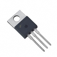
JEDEC TO-220AB
E COLLECTOR (FLANGE) C
G
NOTE: When ordering, use the entire part number. Add the suffix 9A to obtain the TO-263AB and TO-252AA variant in Tape and Reel, e.g., HGT1S2N120CNS9A.
Symbol
C
JEDEC TO-252AA
COLLECTOR (FLANGE)
G
G E E
JEDEC TO-263AB
COLLECTOR (FLANGE) G E
INTERSIL CORPORATION IGBT PRODUCT IS COVERED BY ONE OR MORE OF THE FOLLOWING U.S. PATENTS 4,364,073 4,598,461 4,682,195 4,803,533 4,888,627 4,417,385 4,605,948 4,684,413 4,809,045 4,890,143 4,430,792 4,620,211 4,694,313 4,809,047 4,901,127 4,443,931 4,631,564 4,717,679 4,810,665 4,904,609 4,466,176 4,639,754 4,743,952 4,823,176 4,933,740 4,516,143 4,639,762 4,783,690 4,837,606 4,963,951 4,532,534 4,641,162 4,794,432 4,860,080 4,969,027 4,587,713 4,644,637 4,801,986 4,883,767
1
CAUTION: These devices are sensitive to electrostatic discharge; follow proper ESD Handling Procedures. 1-888-INTERSIL or 321-724-7143 | Copyright © Intersil Corporation 2000 SABER™ is a trademark of Analogy, Inc.
�HGTD2N120CNS, HGTP2N120CN, HGT1S2N120CNS
Absolute Maximum Ratings
TC = 25oC, Unless Otherwise Specified HGTD2N120CNS HGTP2N120CN, HGT1S2N120CNS Collector to Emitter Voltage . . . . . . . . . . . . . . . . . . . . . . . . . . . . . . . . . . . . . . . . . . . . . .BVCES Collector Current Continuous At TC = 25oC . . . . . . . . . . . . . . . . . . . . . . . . . . . . . . . . . . . . . . . . . . . . . . . . . . . . . . . . . IC25 At TC = 110oC . . . . . . . . . . . . . . . . . . . . . . . . . . . . . . . . . . . . . . . . . . . . . . . . . . . . . . . IC110 Collector Current Pulsed (Note 1) . . . . . . . . . . . . . . . . . . . . . . . . . . . . . . . . . . . . . . . . . . . ICM Gate to Emitter Voltage Continuous. . . . . . . . . . . . . . . . . . . . . . . . . . . . . . . . . . . . . . . . . VGES Gate to Emitter Voltage Pulsed . . . . . . . . . . . . . . . . . . . . . . . . . . . . . . . . . . . . . . . . . . . VGEM Switching Safe Operating Area at TJ = 150oC (Figure 2) . . . . . . . . . . . . . . . . . . . . . . . SSOA Power Dissipation Total at TC = 25oC . . . . . . . . . . . . . . . . . . . . . . . . . . . . . . . . . . . . . . . . . PD Power Dissipation Derating TC > 25oC . . . . . . . . . . . . . . . . . . . . . . . . . . . . . . . . . . . . . . . . . . Forward Voltage Avalanche Energy (Note 2) . . . . . . . . . . . . . . . . . . . . . . . . . . . . . . . . . . . EAV Operating and Storage Junction Temperature Range . . . . . . . . . . . . . . . . . . . . . . . . TJ , TSTG Maximum Lead Temperature for Soldering Leads at 0.063in (1.6mm) from case for 10s . . . . . . . . . . . . . . . . . . . . . . . . . . . . . . . . . . TL Package Body for 10s, see Tech Brief 334 . . . . . . . . . . . . . . . . . . . . . . . . . . . . . . . . . .Tpkg Short Circuit Withstand Time (Note 3) at VGE = 15V. . . . . . . . . . . . . . . . . . . . . . . . . . . . . .tSC 1200 13 7 20 ±20 ±30 13A at 1200V 104 0.83 18 -55 to 150 300 260 8
UNITS V A A A V V W W/oC mJ oC
oC oC
µs
CAUTION: Stresses above those listed in “Absolute Maximum Ratings” may cause permanent damage to the device. This is a stress only rating and operation of the device at these or any other conditions above those indicated in the operational sections of this specification is not implied.
NOTES: 1. Pulse width limited by maximum junction temperature. 2. ICE = 3A, L = 4mH. 3. VCE(PK) = 840V, TJ = 125oC, RG = 51Ω .
Electrical Specifications
PARAMETER
TC = 25oC, Unless Otherwise Specified SYMBOL BVCES BVECS ICES TEST CONDITIONS IC = 250µA, VGE = 0V IC = 10mA, VGE = 0V VCE = BVCES TC = 25oC TC = 125oC TC = 150oC MIN 1200 15 6.4 13 TYP 100 2.05 2.75 6.7 10.2 30 36 MAX 100 1.0 2.40 3.50 ±250 36 43 UNITS V V µA µA mA V V V nA A V nC nC
Collector to Emitter Breakdown Voltage Emitter to Collector Breakdown Voltage Collector to Emitter Leakage Current
Collector to Emitter Saturation Voltage
VCE(SAT)
IC = 2.6A, VGE = 15V
TC = 25oC TC = 150oC
Gate to Emitter Threshold Voltage Gate to Emitter Leakage Current Switching SOA Gate to Emitter Plateau Voltage On-State Gate Charge
VGE(TH) IGES SSOA VGEP QG(ON)
IC = 45µA, VCE = VGE VGE = ±20V TJ = 150oC, RG = 51Ω, VGE = 15V, L = 5mH, VCE(PK) = 1200V IC = 2.6A, VCE = 0.5 BVCES IC = 2.6A, VCE = 0.5 BVCES VGE = 15V VGE = 20V
2
�HGTD2N120CNS, HGTP2N120CN, HGT1S2N120CNS
Electrical Specifications
PARAMETER Current Turn-On Delay Time Current Rise Time Current Turn-Off Delay Time Current Fall Time Turn-On Energy (Note 4) Turn-On Energy (Note 4) Turn-Off Energy (Note 5) Current Turn-On Delay Time Current Rise Time Current Turn-Off Delay Time Current Fall Time Turn-On Energy (Note 4) Turn-On Energy (Note 4) Turn-Off Energy (Note 5) Thermal Resistance Junction To Case NOTES: 4. Values for two Turn-On loss conditions are shown for the convenience of the circuit designer. EON1 is the turn-on loss of the IGBT only. EON2 is the turn-on loss when a typical diode is used in the test circuit and the diode is at the same TJ as the IGBT. The diode type is specified in Figure 18. 5. Turn-Off Energy Loss (EOFF) is defined as the integral of the instantaneous power loss starting at the trailing edge of the input pulse and ending at the point where the collector current equals zero (ICE = 0A). All devices were tested per JEDEC Standard No. 24-1 Method for Measurement of Power Device Turn-Off Switching Loss. This test method produces the true total Turn-Off Energy Loss. TC = 25oC, Unless Otherwise Specified (Continued) SYMBOL td(ON)I trI td(OFF)I tfI EON1 EON2 EOFF td(ON)I trI td(OFF)I tfI EON1 EON2 EOFF RθJC IGBT and Diode at TJ = 150oC, ICE = 2.6A, VCE = 0.8 BVCES , VGE = 15V, RG = 51Ω, L = 5mH, Test Circuit (Figure 18) TEST CONDITIONS IGBT and Diode at TJ = 25oC ICE = 2.6A VCE = 0.8 BVCES VGE = 15V RG = 51Ω L = 5mH Test Circuit (Figure 18) MIN TYP 25 11 205 260 96 425 355 21 11 225 360 96 800 530 MAX 30 15 220 320 590 390 25 15 240 420 1100 580 1.20 UNITS ns ns ns ns µJ µJ µJ ns ns ns ns µJ µJ µJ
oC/W
Typical Performance Curves
14 ICE , DC COLLECTOR CURRENT (A)
Unless Otherwise Specified
ICE, COLLECTOR TO EMITTER CURRENT (A)
16 14 12 10 8 6 4 2 0 0
VGE = 15V 12 10 8 6 4 2 0 25 50 75 100 125 150 TC , CASE TEMPERATURE (oC)
TJ = 150oC, RG = 51Ω, VGE = 15V, L = 5mH
200
400
600
800
1000
1200
1400
VCE, COLLECTOR TO EMITTER VOLTAGE (V)
FIGURE 1. DC COLLECTOR CURRENT vs CASE TEMPERATURE
FIGURE 2. MINIMUM SWITCHING SAFE OPERATING AREA
3
�HGTD2N120CNS, HGTP2N120CN, HGT1S2N120CNS Typical Performance Curves
200 fMAX, OPERATING FREQUENCY (kHz)
Unless Otherwise Specified (Continued)
tSC , SHORT CIRCUIT WITHSTAND TIME (µs) ISC , PEAK SHORT CIRCUIT CURRENT (A) 5 5.0 50 VCE = 840V, RG = 51Ω, TJ = 125oC 40 40 50
TJ = 150oC, RG = 51Ω, VGE = 15V, L = 5mH TC = 75oC,VGE = 15V IDEAL DIODE TC VGE 75oC 15V 75oC 12V
100
50
30
30
20 ISC 10 tSC
20
10
fMAX1 = 0.05 / (td(OFF)I + td(ON)I) fMAX2 = (PD - PC) / (EON2 + EOFF) PC = CONDUCTION DISSIPATION (DUTY FACTOR = 50%) RØJC = 1.2oC/W, SEE NOTES 1
TC VGE 110oC 15V oC 12V 110 5
10
0 10 11 12 13 14 15 VGE , GATE TO EMITTER VOLTAGE (V)
0
2 3 4 ICE , COLLECTOR TO EMITTER CURRENT (A)
FIGURE 3. OPERATING FREQUENCY vs COLLECTOR TO EMITTER CURRENT
FIGURE 4. SHORT CIRCUIT WITHSTAND TIME
ICE , COLLECTOR TO EMITTER CURRENT (A)
10
ICE, COLLECTOR TO EMITTER CURRENT (A)
10 DUTY CYCLE