ISL55020
ESIGNS
R NEW D NT
O
F
D
E
E
ND
COMME
PL ACEM r a t
N OT R E
DED RE
N
te
E
n
e
M
Data
Sheet
December 18, 2006
C
M
t
O
por
NO R E C
ical Sup rsil.com/tsc
n
h
c
e
T
r
te
ou
contact ERSIL or www.in
T
N
-I
8
8
1-8
Wideband, Low Distortion, Differential
Amplifier
The ISL55020 is fully differential wideband amplifier
designed to drive differential ADCs. This device features a
high drive capability of 100mA, low operating quiescent
current of 21mA and operates with both single and dual
supplies over a range of 4.5V (±2.25V) to +12V (±6V). Key
features include high impedance, full differential inputs and
full differential or DC referenced complementary singleended outputs A wide bandwidth unity gain common mode
(VCM) amplifier input is included to provide DC offset
correction or common mode signal injection to the
differential output.
FN6287.0
Features
• Fully differential current feedback amplifier
• High impedance differential inputs
• Differential output drives up to 100mA from a +12V supply
• Separate unity-gain common mode input (VCM)
• 300MHz bandwidth
• 1200V/µs Slewrate
• -73.3dBc typical driver output distortion at 10VPP; 1MHz
• -64.6dBc typical driver output distortion at 10VPP; 4MHz
• Low quiescent supply current of 21mA
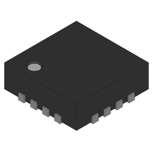
The ISL55020 is available in the thermally-enhanced 16 Ld
QFN package and is specified for operation over the full
-40°C to +85°C temperature range. The ISL55020 has an
EN pin to disable the outputs.
• Pb-free plus anneal available (RoHS compliant)
Ordering Information
• Differential driver
-
16 Ld QFN MDP0046
13”
16 Ld QFN MDP0046
• Wireless communication receiver
• Differential active filter
Pinout
ISL55020
(16 LD QFN)
TOP VIEW
NOTE: Intersil Pb-free plus anneal products employ special Pb-free
material sets; molding compounds/die attach materials and 100%
matte tin plate termination finish, which are RoHS compliant and
compatible with both SnPb and Pb-free soldering operations. Intersil
Pb-free products are MSL classified at Pb-free peak reflow
temperatures that meet or exceed the Pb-free requirements of
IPC/JEDEC J STD-020.
OUT-
PKG.
DWG. #
V+
55020IRZ
ISL55020IRZ-T13 55020IRZ
PACKAGE
(Pb-Free)
NC
TAPE &
REEL
OUT+
16
15
14
13
NC 1
12 NC
+
FB+ 2
11 FB-
+1
+
-
IN+ 3
10 IN-
1
5
6
7
8
EN
9 NC
V-
GND 4
NC
ISL55020IRZ
PART
MARKING
• High Linearity ADC preamplifier
VCM
PART NUMBER
(Note)
Applications
CAUTION: These devices are sensitive to electrostatic discharge; follow proper IC Handling Procedures.
1-888-INTERSIL or 1-888-468-3774 | Intersil (and design) is a registered trademark of Intersil Americas Inc.
Copyright © Intersil Americas Inc. 2006. All Rights Reserved. Elantec is a registered trademark of Elantec Semiconductor, Inc.
All other trademarks mentioned are the property of their respective owners.
�ISL55020
Absolute Maximum Ratings (TA = +25°C)
Thermal Information
V+ Voltage to Ground or V- . . . . . . . . . . . . . . . . . . . -0.3V to +13.2V
V- Voltage to Ground or V+ . . . . . . . . . . . . . . . . . . . +0.3V to -13.2V
IN+, IN-, FB+, FB-, VCM, EN Voltage . . . . . . . V- -0.3V to V+ +0.3V
Current into any Input . . . . . . . . . . . . . . . . . . . . . . . . . . . . . . . . 8mA
Continuous Output Current . . . . . . . . . . . . . . . . . . . . . . . . . . 100mA
ESD Tolerance
Human Body Model . . . . . . . . . . . . . . . . . . . . . . . . . . . . . . . . .3kV
Machine Model . . . . . . . . . . . . . . . . . . . . . . . . . . . . . . . . . . . .200V
Thermal Resistance
JA (°C/W)
16 Ld QFN Package . . . . . . . . . . . . . . . . . . . . . . . .
40
Ambient Operating Temperature Range . . . . . . . . . .-40°C to +85°C
Storage Temperature Range . . . . . . . . . . . . . . . . . .-60°C to +150°C
Operating Junction Temperature . . . . . . . . . . . . . . . . . . . . . . +150°C
CAUTION: Stresses above those listed in “Absolute Maximum Ratings” may cause permanent damage to the device. This is a stress only rating and operation of the
device at these or any other conditions above those indicated in the operational sections of this specification is not implied.
IMPORTANT NOTE: All parameters having Min/Max specifications are guaranteed. Typical values are for information purposes only. Unless otherwise noted, all tests
are at the specified temperature and are pulsed tests, therefore: TJ = TC = TA
Electrical Specifications
VS = 12V, RF = 750, RG = 1.5k, RL = 1k connected to mid supply, TA = +25°C, unless otherwise specified.
PARAMETER
DESCRIPTION
CONDITIONS
MIN
TYP
MAX
UNIT
DC PERFORMANCE
VOS
Common Mode Offset Voltage
-38
15
38
mV
VOS
VOS Mismatch
-7
0.7
7
mV
7
µA
INPUT CHARACTERISTICS
IB+, IB-
Non-Inverting Input Bias Current
-7
FB+, FB-
Inverting Input Bias Current
-125
25
125
µA
IB-
IB- Mismatch
-75
0
75
µA
eN
Input Noise Voltage
iN
CMIR
Input Noise Current
fo = 1kHz
9.8
nV Hz
fo = 10kHz
6.9
nV Hz
fo = 1kHz
6.6
pA/ Hz
fo = 10kHz
2.7
pA/ Hz
Common Mode Input Range IN+, IN-
2
10
V
VCM
IB VCM
VCM Input Bias Current
VCM = 5V to 6V
-7
7
µA
VOS VCM
((VOUT+) + (VOUT -))/2
VCM, IN +, IN- = 0V, RL = 1k
-150
150
mV
VCM Av
Close Loop Gain
VCM = 1V, VCM = 5V to 6V
0.87
1.03
V/V
CMIR
Common Mode Input Range VCM
9.7
V
0.95
2.3
OUTPUT CHARACTERISTICS
VOUT
IOUT
Loaded Output Swing (differential)
Output Current
VS = ±6V, RL = 1kdifferential load
±4.8
VS = 4.5V, RL = 1kdifferential load
±1.05
RL = 0differential load
RL = 50differential load
±5.0
V
V
±150
mA
±1.45
mA
SUPPLY
VS
Supply Voltage
Single supply
4.5
IS+ ENABLE
Positive Supply Current
All outputs at 0V, EN = 0V
14
12
V
21
28
mA
IS- ENABLE
Negative Supply
All outputs at 0V, EN = 0V
-28
-21
-14
mA
IS+ DISABLE
Positive Supply Current
All outputs at 0V, EN = 5V
0.5
1.4
2.5
mA
IS- DISABLE
Negative Supply
All outputs at 0V, EN = 5V
-2.5
-1.6
0.5
mA
Ts
Thermal Shutdown Temperature
IC Junction Temperature
185
°C
Ts-hys
Thermal Shutdown Hysteresis
IC Junction Shutdown Hysteresis
15
°C
2
FN6287.0
December 18, 2006
�ISL55020
Electrical Specifications
VS = 12V, RF = 750, RG = 1.5k, RL = 1k connected to mid supply, TA = +25°C, unless otherwise specified.
(Continued)
PARAMETER
DESCRIPTION
CONDITIONS
MIN
TYP
MAX
UNIT
LOGIC
VINH, EN
ENABLE High Level
VINL, EN
ENABLE Low Level
2
V
V
320
µA
+5
µA
IINH, EN
Input Current, High
ENABLE = 5V
180
IINL, EN
Input Current, Low
ENABLE = 0V
-5
tEN ON
Enable time, off to on
ENABLE = 5V to 0V
12
nS
tEN OFF
Disable time, on to off
ENABLE = 0V to 5V
250
nS
RIN
IN+, IN- Input resistance disables state V+ = 12V, Vin = 2V to 10V, ENABLE = 5V
V+ = 4.5V,Vin = 2V to 4V, ENABLE = 5V
250
0.8
1
M
1
M
AC PERFORMANCE
BW
THD, HD2, HD3
-3dB Bandwidth, single-ended output to AVS = +2.5, RF = 750, RG = 374,
RL=100
GND (Figure 3)
THD, A = 2; Differential
HD2, AV = 2; Differential
HD3, AV = 2; Differential
300
MHz
AVS = 5, RF = 750, RG = 169
RL=100
200
MHz
f = 1MHz, VO = 1VP-P, RL = 1k
-63.8
dBc
f = 1MHz, VO = 10VP-P, RL = 1k
-73.3
dBc
f = 4MHz, VO = 1VP-P, RL = 1k
-57.4
dBc
f = 4MHz, VO = 10VP-P, RL = 1k
-62.4
dBc
f = 1MHz, VO = 1VP-P, RL = 1k
-82.3
dBc
f = 1MHz, VO = 10VP-P, RL = 1k
77.6
dBc
f = 4MHz, VO = 1VP-P, RL = 1k
-62.3
dBc
f = 4MHz, VO = 10VP-P, RL = 1k
-64.6
dBc
f = 1MHz, VO = 1VP-P, RL = 1k
-68.5
dBc
f = 1MHz, VO = 10VP-P, RL = 1k
-83.5
dBc
f = 4MHz, VO = 1VP-P, RL = 1k
-60.3
dBc
f = 4MHz, VO = 10VP-P, RL = 1k
SR
Slew Rate, Single-ended
3
VOUT from -3V to +3V, RL = 1k
600
-67.7
dBc
1200
V/µs
FN6287.0
December 18, 2006
�ISL55020
Typical Performance Curves
1
NORMALIZED GAIN (dB)
0
NORMALIZED GAIN (dB)
-1
RL = 1000
-2
-3
RL = 500
-4
-5
-6
-7
-8
RL = 250
AVS = 2.5
RIN = 200
RF = 750
RG = 374
VOUT = 100mVP-P
-9
100k
1M
RL = 100
RL = 50
10M
100M
1G
16
14
12
10
8
6
4
2
0
-2
AVS = 2.5
-4 R = 200
IN
-6
RF = 750
-8
-10 RG = 374
-12 RL = 100
-14 VOUT = 100mVP-P
-16
100k
1M
35
GAIN (dB)
30
RIN = 200
RL = 100
VOUT = 100mVP-P
25
20
AVS = 5, RF = 750, RG = 169
15
10
AVS = 2.5, RF = 750, RG = 374
5
0
100k
1M
10M
100M
2
VS = ±3
1
0
AVS = 2.5
RIN = 200
RF = 750
RG = 374
RL = 100 to GND
VOUT = 100mVP-P
-1
-2
-3
VS = ±6
1M
10M
100M
NORMALIZED GAIN (dB)
6
RF = 374, RG = 187
2
0
RF = 750, RG = 374
AVS = 2.5
RL= 100
VOUT = 100mVP-P
-10
100k
1M
RF = 1500, RG = 750
10M
100M
-1
-2
-3
-4
-5
-6
-7
-8
1G
FREQUENCY (Hz)
FIGURE 5. SINGLE-ENDED GAIN vs FREQUENCY vs RF/RG
4
RL = 50
RL = 100
RL = 250
RL = 500
RL = 1000
0
8
-2
1G
FIGURE 4. SINGLE-ENDED GAIN vs FREQUENCY vs VS
1
4
1G
FREQUENCY (Hz)
RF = 187, RG = 93.1
10
NORMALIZED GAIN (dB)
100M
3
-5
100k
1G
12
-8
10M
VS = ±2.25
4
-4
FIGURE 3. CLOSED LOOP GAIN vs FREQUENCY
-6
CL = 2.3pF
5
FREQUENCY (Hz)
-4
CL = 9.1pF
FIGURE 2. SINGLE-ENDED GAIN vs FREQUENCY vs CL
NORMALIZED GAIN (dB)
FIGURE 1. SINGLE-ENDED GAIN vs FREQUENCY vs RL
AVS = 50, RF = 750, RG = 15.4
CL = 14.4pF
FREQUENCY (Hz)
FREQUENCY (Hz)
40
C
CLL == 24.3pF
2.3pF
INPUT = VCM
AVCM = 1
AVS = 2.5
RIN = 200
RF = 750
RG = 374
VOUT = 100mVP-P
-9
100k
1M
10M
100M
1G
FREQUENCY (Hz)
FIGURE 6. VCM GAIN vs FREQUENCY vs RL
FN6287.0
December 18, 2006
�ISL55020
Typical Performance Curves (Continued)
1
0
-1
-10
-2
-3
-4
-5
-6
-7
-8
INPUT = VCM
AVCM = 1
AVS = 2.5
RIN = 200
RF = 750
RG = 374
RL = 100
VOUT = 100mVP-P
-9
100k
1M
PSRR+ (dB)
NORMALIZED GAIN (dB)
10
CL = 24.3pF
0
CL = 14.4pF
-20
AVS = 2.5
RIN = 200
RF = 750
RG = 374
RL = 100
VPSRR = 1VP-P
-30
-40
CL = 9.1pF
VS = ±3V
-50
CL = 2.3pF
10M
100M
VS = ±6V
-60
100k
1G
1M
FIGURE 7. VCM GAIN vs FREQUENCY vs CL
10
VS = ±2.25V
VPSRR = 500mVP-P
0
PSRR+ (dB)
PSRR- (dB)
20
-30
-40
VS = ±3V
-10
AVS = 2.5
RIN = 200
RF = 750
RG = 374
RL = 100
VPSRR = 1VP-P
VS = +4.5V
-20 VCM = 2.25V
-40
VS = ±6V
1M
10M
100M
-50
100k
1G
1M
FREQUENCY (Hz)
0
-30
-10
-70
AVS = 2.5
RIN = 200
RF = 1500
RG = 374
RL = 100
VIN = 1VP-P
VCM OFF ISOLATION (dB)
OFF ISOLATION (dB)
-60
-80
-90
-100
-110
-120
100k
100M
1G
FIGURE 10. PSRR+ vs FREQUENCY vs VS (SINGLE SUPPLY)
-20
-50
10M
FREQUENCY (Hz)
FIGURE 9. PSRR- vs FREQUENCY vs VS
-40
1G
-30
-50 VS = ±2.25V
-70
100k
100M
FIGURE 8. PSRR+ vs FREQUENCY vs VS (DUAL SUPPLIES)
10
-60
10M
FREQUENCY (Hz)
FREQUENCY (Hz)
AVS = 2.5
0 RIN = 200
RF = 750
-10 RG = 374
RL = 100
-20 VPSRR = 1VP-P
VS = ±2.25V
-20
-30
-40
-50
-60
AVS = 2.5
AVCM = 1
RIN = 200
RF = 1500
RG = 374
RL = 100
VIN = 1VP-P
-70
-80
-90
-100
1M
10M
100M
1G
FREQUENCY (Hz)
FIGURE 11. INPUT OFF ISOLATION GAIN vs FREQUENCY
SINGLE-ENDED
5
-110
100k
1M
10M
100M
1G
FREQUENCY (Hz)
FIGURE 12. VCM OFF ISOLATION vs FREQUENCY - SINGLEENDED
FN6287.0
December 18, 2006
�ISL55020
Typical Performance Curves (Continued)
0.12
6
0.10
4
VOUT (V)
VOUT (V)
0.08
0.06
0.04
2
0
-2
0.02
AVS = 2.5
VS = ±6V
RL = 100 TO GND
0
-0.02
0
5
10
15
20
25
AVS = 2.5
VS = ±6V
RL = 100 TO GND
-4
30
35
40
45
-6
50
0
50
100
150
TIME (ns)
0.12
3
0.10
2
0.08
1
0.06
0.04
350
400
0
-1
-2
0.02
AVS = 2.5
VS = ±6V
RL = 100 TO GND
0
-0.02
300
FIGURE 14. LARGE SIGNAL STEP RESPONSE
VOUT (V)
VOUT (V)
FIGURE 13. SMALL SIGNAL STEP RESPONSE
200
250
TIME (ns)
0
5
10
15
20
25
30
AVS = 2.5
VS = ±6V
RL = 100 TO GND
-3
-4
35
40
45
50
0
50
100
150
200
250
300
350
400
TIME (ns)
TIME (ns)
FIGURE 16. LARGE SIGNAL STEP RESPONSE - VCM TO
VOUT
FIGURE 15. SMALL SIGNAL STEP RESPONSE - VCM TO
VOUT
2.1
6
V-ENABLE (V)
1.8
5
4
AVS = 2.5
VS = ±6V
RL = 100 TO GND
1.2
0.9
3
2
0.6
1
0.3
0
0
VOUT (V)
0
100
200
300
400
500
TIME (ns)
V-ENABLE (V)
VOUT (V)
1.5
600
700
-1
800
FIGURE 17. ENABLE TO OUTPUT DELAY
6
FN6287.0
December 18, 2006
�ISL55020
Pin Descriptions
EQUIVALENT
CIRCUIT
PIN NUMBER
PIN NAME
PIN FUNCTION
1, 6, 9, 12, 15
NC
2
FB+
Circuit1
Feedback from non-inverting output
3
IN+
Circuit 1
Non-inverting input
4
GND
Circuit 4
Ground
5
VCM
Circuit 1
Reference input, sets common-mode output voltage with AV = 1. Must be st to
V+/2 for single supply applications
7
V-
Circuit 4
Negative supply. Must be connected to GND for single supply operation
8
EN
Circuit 2
Enable pin with internal pull-down; Logic “1” selects the disabled state; Logic “0”
selects the enabled state
10
IN-
Circuit 1
Inverting input
11
FB-
Circuit 1
Feedback from inverting output
13
OUT-
Circuit 3
Inverting output
14
V+
Circuit 4
Positive supply
16
OUT+
Circuit 3
Non-inverting output
Circuit 5
Pack thermal pad electrically connected to IC substrate - must be connected to
most negative voltage applied to the IC
No connect; grounded for best AC performance
Thermal Pad
V+
FB+,FB-
IN+, INVCM
EN
V-
V+
V+
GND
OUT
V-
VCIRCUIT 2
CIRCUIT 1
CIRCUIT 3
THERMAL HEAT SINK PAD
V+
CAPACITIVELY
COUPLED
ESD CLAMP
GND
~1M
VSUBSTRATE
VCIRCUIT 4.
7
CIRCUIT 5
FN6287.0
December 18, 2006
�ISL55020
V+
V-
RF1
RIN+
VIN+
RT+
RG
RTVCM
V+
V-
OUT+
RS+
RL+
VOUT+
VCM +1
RIN-
VIN-
FB+
IN+
INFB-
RT-VCM
GNDOUTEN
RS+
RL-
VOUT -
RF2
EN
GND-
FIGURE 18. BASIC APPLICATION CIRCUIT
Description of Operation and Application
Information
Product Description
mode signal is outside the above-specified ranges, the
output signal will be distorted.
The output of the ISL55020 can swing from -3.8V to +3.8V at
100 differential load at ±5V supply. As the load resistance
becomes lower, the output swing is reduced.
The ISL55020 is a full differential Current Feedback
Amplifier (CFA) featuring wide bandwidth and low power.
The device contains a pair of high impedance differential
inputs and a pair of differential outputs. It can be used in any
combination of single/differential ended input/output
configurations. A wide bandwidth unity gain, common mode
amplifier with a 100MHz -3dB bandwidth (Figure 6) is
included to provide DC offset correction or common mode
signal injection to the differential output. The ISL55020 is
internally compensated for single-ended closed loop gain
(AVS), differential closed gain (AVD) of 2, or greater.
Connected in differential gain of 5 (single ended gain of ±2.5
and driving a 200 differential load, the ISL55020 has a 3dB bandwidth of 300MHz. Driving a 200 differential load
at gain of 10, the bandwidth is about 200MHz (Figure 3). The
ISL55020 is available with a power down feature (EN) to
reduce the power while the amplifier is disabled.
The differential output gain (AVD) is defined by the feedback
resistors according to the following
Input, Output, and Supply Voltage Range
AVD = 1 + 2RF/RG
The ISL55020 is designed to operate with dual supplies over
a range of +/-2.25V to +/-6V and can also operate with a
single supply over the range of 4.5V to 12V. For single
supply operation, the V- and GND pins must be connected
together as close to the device as possible. The amplifiers
have an input common mode voltage range from -4.3V to
3.4V when operated from ±5V supplies. The differential
mode input range (DMIR) between the two inputs is from 2.3V to +2.3V. The input voltage range at the VCM pin is
from -3.3V to 3.7V. If the input common mode or differential
8
Single-ended, Differential and Common Mode Gain
Settings
The ISL55020 can be used as a single/differential ended to
differential/single converter. The voltage applied at VCM pin
sets the output common mode voltage and the common
mode gain is fixed at gain is one (AVCM = 1).
The output differential voltage is given by the following:
VOD = (VIN+ - VIN-) x (1 + 2RF/RG)
(EQ. 1)
Where:
RF1 = RF2 = RF
(EQ. 2)
The single ended output voltage (VOS) contains a common
mode component (VCM) and a differential mode component
equal to one-half the differential output (VOD/2)., and is
given by the following:
VOS = VOD/2 + VCM = VCM +(VIN+ - VIN-) x (0.5 + RF/RG) (EQ. 3)
and the single-ended gain becomes:
AVS = 0.5+ RF/RG
(EQ. 4)
FN6287.0
December 18, 2006
�ISL55020
Feedback Resistor, Gain Bandwidth Product and
Stability Considerations (See Figure 18 - Basic
Application Schematic)
For gains greater than 1, the feedback resistor forms a pole
with the parasitic capacitance at the inverting input. As this
pole becomes lower in frequency, the amplifier's phase
margin is reduced. Excessive parasitic capacitance at the
input will cause excessive ringing in the time domain and
peaking in the frequency domain. High feedback resistor
values have the same effect, and therefore should be kept
as low as possible. Figure 5 shows the gain-peaking effect of
using higher feedback resistor values. Feedback resistor RF
has some maximum value that should not be exceeded for
optimum performance.
Unlike voltage feedback (VFA) amplifier topologies that
exhibit constant gain-bandwidth product, CFA amplifiers
maintain high bandwidth at gains high greater than 1.
Figure 3 illustrates the nearly constant bandwidth from a
single-ended gain (AVS) of 2.5 to 5, and only a slight
reduction out to a AVS of 50. For the gains other than 1,
optimum response is obtained with RF between 500 to
1k.
Output Drive Capability
The ISL55020 has no internal current-limiting circuitry. If the
output is shorted, it is possible to exceed the Absolute
Maximum Rating for output current or power dissipation,
potentially resulting in the destruction of the device.internal
short circuit protection.
Power Dissipation
With the high output drive capability of the ISL55020, It is
possible to exceed the +150°C absolute maximum junction
temperature under certain load current conditions.
Therefore, it is important to calculate the maximum junction
temperature for the application to determine if the load
conditions or package types need to be modified for the
amplifier to remain in the safe operating area.
A thermal shutdown circuit is included that implements a
thermal shutdown if the junction temperature exceeds
~+185°C. The thermal shutdown includes thermal hysteresis
of ~+15°C. The thermal shutdown feature is designed to
protect the device during accidental overload conditions and
continuous operation at junction temperatures greater than
+150°C should never be allowed.
The high impedance inputs IN+ and IN- are sensitive
parasitic capacitance and inductance. To ensure input
stability, a small value resistor (200 recommended) should
be placed as close to the device IN+ and IN- pins as
possible.
The maximum power dissipation allowed in a package is
determined according to:
Driving Capacitive Loads and Cables
Where:
Excessive output capacitance also contributes to gain
peaking (Figure 2) and high overshoot in pulse applications.
For PC board layouts requiring long traces at the output, a
small series resistor (Figure 17 - RS+, RS- usually between
5 to 50should be inserted as close to the device output
pin as possible to each to minimize peaking,. The resultant
gain error should be compensated with an appropriate
adjustment of RG.
When used as a cable driver, double termination is always
recommended for reflection-free performance. For those
applications, a back-termination series resistor (RS) at the
amplifier's output will isolate the amplifier from the cable and
allow extensive capacitive drive. However, other applications
may have high capacitive loads without a back-termination
resistor. Again, a small series resistor at the output can help
to reduce peaking.
Disable/Power-Down
The ISL55020 can be disabled with it’s outputs in a high
impedance state. The turn off time is about 250nS and the
turn on time is about 12nS (Figure 17). When disabled, the
amplifier's supply current is reduced to 1.4mA for IS+ and 1.6mA for IS- typically. The amplifier's power down can be
controlled by standard ground-referenced CMOS signal
levels at the EN pin. V.
9
T JMAX – T AMAX
PD MAX = -------------------------------------------- JA
TJMAX = Maximum junction temperature
TAMAX = Maximum ambient temperature
JA = Thermal resistance of the package
The maximum power dissipation actually produced by an IC
is the total quiescent supply current times the total power
supply voltage, plus the power in the IC due to the load, or:
V O
PD = V S I SMAX + V S -----------R
LD
Where:
VS = Total supply voltage
ISMAX = Maximum quiescent supply current per channel
VO = Maximum differential output voltage of the
application
RLD = Differential load resistance
ILOAD = Load current
By setting the two PDMAX equations equal to each other, we
can solve the output current and RLD to avoid the device
overheat.
FN6287.0
December 18, 2006
�ISL55020
Power Supply Bypassing and Printed Circuit
Board Layout
As with any high frequency device, a good printed circuit
board layout is necessary for optimum performance. Lead
lengths should be as sort as possible. The power supply pin
must be well bypassed to reduce the risk of oscillation. For
normal single supply operation, where the V- pin is
connected to the ground plane, a single 4.7µF tantalum
capacitor in parallel with a 0.1µF ceramic capacitor from V+
to GND will suffice. This same capacitor combination should
be placed at each supply pin to ground if split supplies are to
be used. In this case, the V- pin becomes the negative
supply rail.
For good AC performance, parasitic capacitance should be
kept to minimum. Use of wire wound resistors should be
avoided because of their additional series inductance. Use
of sockets should also be avoided if possible. Sockets add
parasitic inductance and capacitance that can result in
compromised performance. Minimizing parasitic capacitance
at the amplifier's inverting input pin is very important. The
feedback resistor should be placed very close to the
inverting input pin. Strip line design techniques are
recommended for the signal traces.
For additional products, see www.intersil.com/en/products.html
Intersil products are manufactured, assembled and tested utilizing ISO9001 quality systems as noted
in the quality certifications found at www.intersil.com/en/support/qualandreliability.html
Intersil products are sold by description only. Intersil Corporation reserves the right to make changes in circuit design, software and/or specifications at any time
without notice. Accordingly, the reader is cautioned to verify that data sheets are current before placing orders. Information furnished by Intersil is believed to be
accurate and reliable. However, no responsibility is assumed by Intersil or its subsidiaries for its use; nor for any infringements of patents or other rights of third
parties which may result from its use. No license is granted by implication or otherwise under any patent or patent rights of Intersil or its subsidiaries.
For information regarding Intersil Corporation and its products, see www.intersil.com
10
FN6287.0
December 18, 2006
�ISL55020
QFN (Quad Flat No-Lead) Package Family
QFN (QUAD FLAT NO-LEAD) PACKAGE FAMILY
(COMPLIANT TO JEDEC MO-220)
A
SYMBOL QFN44 QFN38
D
B
N
(N-1)
(N-2)
1
2
3
PIN #1
I.D. MARK
E
(N/2)
2X
0.075 C
2X
0.075 C
N LEADS
TOP VIEW
QFN32
TOLERANCE
NOTES
A
0.90
0.90
0.90
0.90
±0.10
-
A1
0.02
0.02
0.02
0.02
+0.03/-0.02
-
b
0.25
0.25
0.23
0.22
±0.02
-
c
0.20
0.20
0.20
0.20
Reference
-
D
7.00
5.00
8.00
5.00
D2
5.10
3.80
5.80 3.60/2.48
E
7.00
7.00
8.00
E2
5.10
5.80
5.80 4.60/3.40
e
0.50
0.50
0.80
L
0.55
0.40
0.53
Basic
-
Reference
8
6.00
Basic
-
Reference
8
0.50
Basic
-
0.50
±0.05
-
N
44
38
32
32
Reference
4
ND
11
7
8
7
Reference
6
NE
11
12
8
9
Reference
5
0.10 M C A B
(N-2)
(N-1)
N
b
L
PIN #1 I.D.
3
1
2
3
(E2)
(N/2)
NE 5
7
(D2)
BOTTOM VIEW
0.10 C
e
C
SYMBOL QFN28 QFN24
QFN20
QFN16
TOLERANCE NOTES
A
0.90
0.90
0.90
0.90
0.90
±0.10
-
A1
0.02
0.02
0.02
0.02
0.02
+0.03/
-0.02
-
b
0.25
0.25
0.30
0.25
0.33
±0.02
-
c
0.20
0.20
0.20
0.20
0.20
Reference
-
D
4.00
4.00
5.00
4.00
4.00
Basic
-
D2
2.65
2.80
3.70
2.70
2.40
Reference
-
E
5.00
5.00
5.00
4.00
4.00
Basic
-
E2
3.65
3.80
3.70
2.70
2.40
Reference
-
e
0.50
0.50
0.65
0.50
0.65
Basic
-
L
0.40
0.40
0.40
0.40
0.60
±0.05
-
N
28
24
20
20
16
Reference
4
ND
6
5
5
5
4
Reference
6
NE
8
7
5
5
4
Reference
5
Rev 10 12/04
SEATING
PLANE
NOTES:
0.08 C
N LEADS
& EXPOSED PAD
SEE DETAIL "X"
(c)
5. NE is the number of terminals on the “E” side of the package
(or Y-direction).
6. ND is the number of terminals on the “D” side of the package
(or X-direction). ND = (N/2)-NE.
(L)
A1
N LEADS
DETAIL X
11
2. Tiebar view shown is a non-functional feature.
4. N is the total number of terminals on the device.
2
A
1. Dimensioning and tolerancing per ASME Y14.5M-1994.
3. Bottom-side pin #1 I.D. is a diepad chamfer as shown.
SIDE VIEW
C
MDP0046
7. Inward end of terminal may be square or circular in shape with radius
(b/2) as shown.
8. If two values are listed, multiple exposed pad options are available.
Refer to device-specific datasheet.
FN6287.0
December 18, 2006
�ISL55020
ESIGNS
R NEW D NT
O
F
D
E
E
ND
COMME
PL ACEM r a t
N OT R E
DED RE
N
te
E
n
e
M
Data
Sheet
December 18, 2006
C
M
t
O
por
NO R E C
ical Sup rsil.com/tsc
n
h
c
e
T
r
te
ou
contact ERSIL or www.in
T
N
-I
8
8
1-8
Wideband, Low Distortion, Differential
Amplifier
The ISL55020 is fully differential wideband amplifier
designed to drive differential ADCs. This device features a
high drive capability of 100mA, low operating quiescent
current of 21mA and operates with both single and dual
supplies over a range of 4.5V (±2.25V) to +12V (±6V). Key
features include high impedance, full differential inputs and
full differential or DC referenced complementary singleended outputs A wide bandwidth unity gain common mode
(VCM) amplifier input is included to provide DC offset
correction or common mode signal injection to the
differential output.
FN6287.0
Features
• Fully differential current feedback amplifier
• High impedance differential inputs
• Differential output drives up to 100mA from a +12V supply
• Separate unity-gain common mode input (VCM)
• 300MHz bandwidth
• 1200V/µs Slewrate
• -73.3dBc typical driver output distortion at 10VPP; 1MHz
• -64.6dBc typical driver output distortion at 10VPP; 4MHz
• Low quiescent supply current of 21mA
The ISL55020 is available in the thermally-enhanced 16 Ld
QFN package and is specified for operation over the full
-40°C to +85°C temperature range. The ISL55020 has an
EN pin to disable the outputs.
• Pb-free plus anneal available (RoHS compliant)
Ordering Information
• Differential driver
-
16 Ld QFN MDP0046
13”
16 Ld QFN MDP0046
• Wireless communication receiver
• Differential active filter
Pinout
ISL55020
(16 LD QFN)
TOP VIEW
NOTE: Intersil Pb-free plus anneal products employ special Pb-free
material sets; molding compounds/die attach materials and 100%
matte tin plate termination finish, which are RoHS compliant and
compatible with both SnPb and Pb-free soldering operations. Intersil
Pb-free products are MSL classified at Pb-free peak reflow
temperatures that meet or exceed the Pb-free requirements of
IPC/JEDEC J STD-020.
OUT-
PKG.
DWG. #
V+
55020IRZ
ISL55020IRZ-T13 55020IRZ
PACKAGE
(Pb-Free)
NC
TAPE &
REEL
OUT+
16
15
14
13
NC 1
12 NC
+
FB+ 2
11 FB-
+1
+
-
IN+ 3
10 IN-
1
5
6
7
8
EN
9 NC
V-
GND 4
NC
ISL55020IRZ
PART
MARKING
• High Linearity ADC preamplifier
VCM
PART NUMBER
(Note)
Applications
CAUTION: These devices are sensitive to electrostatic discharge; follow proper IC Handling Procedures.
1-888-INTERSIL or 1-888-468-3774 | Intersil (and design) is a registered trademark of Intersil Americas Inc.
Copyright © Intersil Americas Inc. 2006. All Rights Reserved. Elantec is a registered trademark of Elantec Semiconductor, Inc.
All other trademarks mentioned are the property of their respective owners.
�ISL55020
Absolute Maximum Ratings (TA = +25°C)
Thermal Information
V+ Voltage to Ground or V- . . . . . . . . . . . . . . . . . . . -0.3V to +13.2V
V- Voltage to Ground or V+ . . . . . . . . . . . . . . . . . . . +0.3V to -13.2V
IN+, IN-, FB+, FB-, VCM, EN Voltage . . . . . . . V- -0.3V to V+ +0.3V
Current into any Input . . . . . . . . . . . . . . . . . . . . . . . . . . . . . . . . 8mA
Continuous Output Current . . . . . . . . . . . . . . . . . . . . . . . . . . 100mA
ESD Tolerance
Human Body Model . . . . . . . . . . . . . . . . . . . . . . . . . . . . . . . . .3kV
Machine Model . . . . . . . . . . . . . . . . . . . . . . . . . . . . . . . . . . . .200V
Thermal Resistance
JA (°C/W)
16 Ld QFN Package . . . . . . . . . . . . . . . . . . . . . . . .
40
Ambient Operating Temperature Range . . . . . . . . . .-40°C to +85°C
Storage Temperature Range . . . . . . . . . . . . . . . . . .-60°C to +150°C
Operating Junction Temperature . . . . . . . . . . . . . . . . . . . . . . +150°C
CAUTION: Stresses above those listed in “Absolute Maximum Ratings” may cause permanent damage to the device. This is a stress only rating and operation of the
device at these or any other conditions above those indicated in the operational sections of this specification is not implied.
IMPORTANT NOTE: All parameters having Min/Max specifications are guaranteed. Typical values are for information purposes only. Unless otherwise noted, all tests
are at the specified temperature and are pulsed tests, therefore: TJ = TC = TA
Electrical Specifications
VS = 12V, RF = 750, RG = 1.5k, RL = 1k connected to mid supply, TA = +25°C, unless otherwise specified.
PARAMETER
DESCRIPTION
CONDITIONS
MIN
TYP
MAX
UNIT
DC PERFORMANCE
VOS
Common Mode Offset Voltage
-38
15
38
mV
VOS
VOS Mismatch
-7
0.7
7
mV
7
µA
INPUT CHARACTERISTICS
IB+, IB-
Non-Inverting Input Bias Current
-7
FB+, FB-
Inverting Input Bias Current
-125
25
125
µA
IB-
IB- Mismatch
-75
0
75
µA
eN
Input Noise Voltage
iN
CMIR
Input Noise Current
fo = 1kHz
9.8
nV Hz
fo = 10kHz
6.9
nV Hz
fo = 1kHz
6.6
pA/ Hz
fo = 10kHz
2.7
pA/ Hz
Common Mode Input Range IN+, IN-
2
10
V
VCM
IB VCM
VCM Input Bias Current
VCM = 5V to 6V
-7
7
µA
VOS VCM
((VOUT+) + (VOUT -))/2
VCM, IN +, IN- = 0V, RL = 1k
-150
150
mV
VCM Av
Close Loop Gain
VCM = 1V, VCM = 5V to 6V
0.87
1.03
V/V
CMIR
Common Mode Input Range VCM
9.7
V
0.95
2.3
OUTPUT CHARACTERISTICS
VOUT
IOUT
Loaded Output Swing (differential)
Output Current
VS = ±6V, RL = 1kdifferential load
±4.8
VS = 4.5V, RL = 1kdifferential load
±1.05
RL = 0differential load
RL = 50differential load
±5.0
V
V
±150
mA
±1.45
mA
SUPPLY
VS
Supply Voltage
Single supply
4.5
IS+ ENABLE
Positive Supply Current
All outputs at 0V, EN = 0V
14
12
V
21
28
mA
IS- ENABLE
Negative Supply
All outputs at 0V, EN = 0V
-28
-21
-14
mA
IS+ DISABLE
Positive Supply Current
All outputs at 0V, EN = 5V
0.5
1.4
2.5
mA
IS- DISABLE
Negative Supply
All outputs at 0V, EN = 5V
-2.5
-1.6
0.5
mA
Ts
Thermal Shutdown Temperature
IC Junction Temperature
185
°C
Ts-hys
Thermal Shutdown Hysteresis
IC Junction Shutdown Hysteresis
15
°C
2
FN6287.0
December 18, 2006
�ISL55020
Electrical Specifications
VS = 12V, RF = 750, RG = 1.5k, RL = 1k connected to mid supply, TA = +25°C, unless otherwise specified.
(Continued)
PARAMETER
DESCRIPTION
CONDITIONS
MIN
TYP
MAX
UNIT
LOGIC
VINH, EN
ENABLE High Level
VINL, EN
ENABLE Low Level
2
V
V
320
µA
+5
µA
IINH, EN
Input Current, High
ENABLE = 5V
180
IINL, EN
Input Current, Low
ENABLE = 0V
-5
tEN ON
Enable time, off to on
ENABLE = 5V to 0V
12
nS
tEN OFF
Disable time, on to off
ENABLE = 0V to 5V
250
nS
RIN
IN+, IN- Input resistance disables state V+ = 12V, Vin = 2V to 10V, ENABLE = 5V
V+ = 4.5V,Vin = 2V to 4V, ENABLE = 5V
250
0.8
1
M
1
M
AC PERFORMANCE
BW
THD, HD2, HD3
-3dB Bandwidth, single-ended output to AVS = +2.5, RF = 750, RG = 374,
RL=100
GND (Figure 3)
THD, A = 2; Differential
HD2, AV = 2; Differential
HD3, AV = 2; Differential
300
MHz
AVS = 5, RF = 750, RG = 169
RL=100
200
MHz
f = 1MHz, VO = 1VP-P, RL = 1k
-63.8
dBc
f = 1MHz, VO = 10VP-P, RL = 1k
-73.3
dBc
f = 4MHz, VO = 1VP-P, RL = 1k
-57.4
dBc
f = 4MHz, VO = 10VP-P, RL = 1k
-62.4
dBc
f = 1MHz, VO = 1VP-P, RL = 1k
-82.3
dBc
f = 1MHz, VO = 10VP-P, RL = 1k
77.6
dBc
f = 4MHz, VO = 1VP-P, RL = 1k
-62.3
dBc
f = 4MHz, VO = 10VP-P, RL = 1k
-64.6
dBc
f = 1MHz, VO = 1VP-P, RL = 1k
-68.5
dBc
f = 1MHz, VO = 10VP-P, RL = 1k
-83.5
dBc
f = 4MHz, VO = 1VP-P, RL = 1k
-60.3
dBc
f = 4MHz, VO = 10VP-P, RL = 1k
SR
Slew Rate, Single-ended
3
VOUT from -3V to +3V, RL = 1k
600
-67.7
dBc
1200
V/µs
FN6287.0
December 18, 2006
�ISL55020
Typical Performance Curves
1
NORMALIZED GAIN (dB)
0
NORMALIZED GAIN (dB)
-1
RL = 1000
-2
-3
RL = 500
-4
-5
-6
-7
-8
RL = 250
AVS = 2.5
RIN = 200
RF = 750
RG = 374
VOUT = 100mVP-P
-9
100k
1M
RL = 100
RL = 50
10M
100M
1G
16
14
12
10
8
6
4
2
0
-2
AVS = 2.5
-4 R = 200
IN
-6
RF = 750
-8
-10 RG = 374
-12 RL = 100
-14 VOUT = 100mVP-P
-16
100k
1M
35
GAIN (dB)
30
RIN = 200
RL = 100
VOUT = 100mVP-P
25
20
AVS = 5, RF = 750, RG = 169
15
10
AVS = 2.5, RF = 750, RG = 374
5
0
100k
1M
10M
100M
2
VS = ±3
1
0
AVS = 2.5
RIN = 200
RF = 750
RG = 374
RL = 100 to GND
VOUT = 100mVP-P
-1
-2
-3
VS = ±6
1M
10M
100M
NORMALIZED GAIN (dB)
6
RF = 374, RG = 187
2
0
RF = 750, RG = 374
AVS = 2.5
RL= 100
VOUT = 100mVP-P
-10
100k
1M
RF = 1500, RG = 750
10M
100M
-1
-2
-3
-4
-5
-6
-7
-8
1G
FREQUENCY (Hz)
FIGURE 5. SINGLE-ENDED GAIN vs FREQUENCY vs RF/RG
4
RL = 50
RL = 100
RL = 250
RL = 500
RL = 1000
0
8
-2
1G
FIGURE 4. SINGLE-ENDED GAIN vs FREQUENCY vs VS
1
4
1G
FREQUENCY (Hz)
RF = 187, RG = 93.1
10
NORMALIZED GAIN (dB)
100M
3
-5
100k
1G
12
-8
10M
VS = ±2.25
4
-4
FIGURE 3. CLOSED LOOP GAIN vs FREQUENCY
-6
CL = 2.3pF
5
FREQUENCY (Hz)
-4
CL = 9.1pF
FIGURE 2. SINGLE-ENDED GAIN vs FREQUENCY vs CL
NORMALIZED GAIN (dB)
FIGURE 1. SINGLE-ENDED GAIN vs FREQUENCY vs RL
AVS = 50, RF = 750, RG = 15.4
CL = 14.4pF
FREQUENCY (Hz)
FREQUENCY (Hz)
40
C
CLL == 24.3pF
2.3pF
INPUT = VCM
AVCM = 1
AVS = 2.5
RIN = 200
RF = 750
RG = 374
VOUT = 100mVP-P
-9
100k
1M
10M
100M
1G
FREQUENCY (Hz)
FIGURE 6. VCM GAIN vs FREQUENCY vs RL
FN6287.0
December 18, 2006
�ISL55020
Typical Performance Curves (Continued)
1
0
-1
-10
-2
-3
-4
-5
-6
-7
-8
INPUT = VCM
AVCM = 1
AVS = 2.5
RIN = 200
RF = 750
RG = 374
RL = 100
VOUT = 100mVP-P
-9
100k
1M
PSRR+ (dB)
NORMALIZED GAIN (dB)
10
CL = 24.3pF
0
CL = 14.4pF
-20
AVS = 2.5
RIN = 200
RF = 750
RG = 374
RL = 100
VPSRR = 1VP-P
-30
-40
CL = 9.1pF
VS = ±3V
-50
CL = 2.3pF
10M
100M
VS = ±6V
-60
100k
1G
1M
FIGURE 7. VCM GAIN vs FREQUENCY vs CL
10
VS = ±2.25V
VPSRR = 500mVP-P
0
PSRR+ (dB)
PSRR- (dB)
20
-30
-40
VS = ±3V
-10
AVS = 2.5
RIN = 200
RF = 750
RG = 374
RL = 100
VPSRR = 1VP-P
VS = +4.5V
-20 VCM = 2.25V
-40
VS = ±6V
1M
10M
100M
-50
100k
1G
1M
FREQUENCY (Hz)
0
-30
-10
-70
AVS = 2.5
RIN = 200
RF = 1500
RG = 374
RL = 100
VIN = 1VP-P
VCM OFF ISOLATION (dB)
OFF ISOLATION (dB)
-60
-80
-90
-100
-110
-120
100k
100M
1G
FIGURE 10. PSRR+ vs FREQUENCY vs VS (SINGLE SUPPLY)
-20
-50
10M
FREQUENCY (Hz)
FIGURE 9. PSRR- vs FREQUENCY vs VS
-40
1G
-30
-50 VS = ±2.25V
-70
100k
100M
FIGURE 8. PSRR+ vs FREQUENCY vs VS (DUAL SUPPLIES)
10
-60
10M
FREQUENCY (Hz)
FREQUENCY (Hz)
AVS = 2.5
0 RIN = 200
RF = 750
-10 RG = 374
RL = 100
-20 VPSRR = 1VP-P
VS = ±2.25V
-20
-30
-40
-50
-60
AVS = 2.5
AVCM = 1
RIN = 200
RF = 1500
RG = 374
RL = 100
VIN = 1VP-P
-70
-80
-90
-100
1M
10M
100M
1G
FREQUENCY (Hz)
FIGURE 11. INPUT OFF ISOLATION GAIN vs FREQUENCY
SINGLE-ENDED
5
-110
100k
1M
10M
100M
1G
FREQUENCY (Hz)
FIGURE 12. VCM OFF ISOLATION vs FREQUENCY - SINGLEENDED
FN6287.0
December 18, 2006
�ISL55020
Typical Performance Curves (Continued)
0.12
6
0.10
4
VOUT (V)
VOUT (V)
0.08
0.06
0.04
2
0
-2
0.02
AVS = 2.5
VS = ±6V
RL = 100 TO GND
0
-0.02
0
5
10
15
20
25
AVS = 2.5
VS = ±6V
RL = 100 TO GND
-4
30
35
40
45
-6
50
0
50
100
150
TIME (ns)
0.12
3
0.10
2
0.08
1
0.06
0.04
350
400
0
-1
-2
0.02
AVS = 2.5
VS = ±6V
RL = 100 TO GND
0
-0.02
300
FIGURE 14. LARGE SIGNAL STEP RESPONSE
VOUT (V)
VOUT (V)
FIGURE 13. SMALL SIGNAL STEP RESPONSE
200
250
TIME (ns)
0
5
10
15
20
25
30
AVS = 2.5
VS = ±6V
RL = 100 TO GND
-3
-4
35
40
45
50
0
50
100
150
200
250
300
350
400
TIME (ns)
TIME (ns)
FIGURE 16. LARGE SIGNAL STEP RESPONSE - VCM TO
VOUT
FIGURE 15. SMALL SIGNAL STEP RESPONSE - VCM TO
VOUT
2.1
6
V-ENABLE (V)
1.8
5
4
AVS = 2.5
VS = ±6V
RL = 100 TO GND
1.2
0.9
3
2
0.6
1
0.3
0
0
VOUT (V)
0
100
200
300
400
500
TIME (ns)
V-ENABLE (V)
VOUT (V)
1.5
600
700
-1
800
FIGURE 17. ENABLE TO OUTPUT DELAY
6
FN6287.0
December 18, 2006
�ISL55020
Pin Descriptions
EQUIVALENT
CIRCUIT
PIN NUMBER
PIN NAME
PIN FUNCTION
1, 6, 9, 12, 15
NC
2
FB+
Circuit1
Feedback from non-inverting output
3
IN+
Circuit 1
Non-inverting input
4
GND
Circuit 4
Ground
5
VCM
Circuit 1
Reference input, sets common-mode output voltage with AV = 1. Must be st to
V+/2 for single supply applications
7
V-
Circuit 4
Negative supply. Must be connected to GND for single supply operation
8
EN
Circuit 2
Enable pin with internal pull-down; Logic “1” selects the disabled state; Logic “0”
selects the enabled state
10
IN-
Circuit 1
Inverting input
11
FB-
Circuit 1
Feedback from inverting output
13
OUT-
Circuit 3
Inverting output
14
V+
Circuit 4
Positive supply
16
OUT+
Circuit 3
Non-inverting output
Circuit 5
Pack thermal pad electrically connected to IC substrate - must be connected to
most negative voltage applied to the IC
No connect; grounded for best AC performance
Thermal Pad
V+
FB+,FB-
IN+, INVCM
EN
V-
V+
V+
GND
OUT
V-
VCIRCUIT 2
CIRCUIT 1
CIRCUIT 3
THERMAL HEAT SINK PAD
V+
CAPACITIVELY
COUPLED
ESD CLAMP
GND
~1M
VSUBSTRATE
VCIRCUIT 4.
7
CIRCUIT 5
FN6287.0
December 18, 2006
�ISL55020
V+
V-
RF1
RIN+
VIN+
RT+
RG
RTVCM
V+
V-
OUT+
RS+
RL+
VOUT+
VCM +1
RIN-
VIN-
FB+
IN+
INFB-
RT-VCM
GNDOUTEN
RS+
RL-
VOUT -
RF2
EN
GND-
FIGURE 18. BASIC APPLICATION CIRCUIT
Description of Operation and Application
Information
Product Description
mode signal is outside the above-specified ranges, the
output signal will be distorted.
The output of the ISL55020 can swing from -3.8V to +3.8V at
100 differential load at ±5V supply. As the load resistance
becomes lower, the output swing is reduced.
The ISL55020 is a full differential Current Feedback
Amplifier (CFA) featuring wide bandwidth and low power.
The device contains a pair of high impedance differential
inputs and a pair of differential outputs. It can be used in any
combination of single/differential ended input/output
configurations. A wide bandwidth unity gain, common mode
amplifier with a 100MHz -3dB bandwidth (Figure 6) is
included to provide DC offset correction or common mode
signal injection to the differential output. The ISL55020 is
internally compensated for single-ended closed loop gain
(AVS), differential closed gain (AVD) of 2, or greater.
Connected in differential gain of 5 (single ended gain of ±2.5
and driving a 200 differential load, the ISL55020 has a 3dB bandwidth of 300MHz. Driving a 200 differential load
at gain of 10, the bandwidth is about 200MHz (Figure 3). The
ISL55020 is available with a power down feature (EN) to
reduce the power while the amplifier is disabled.
The differential output gain (AVD) is defined by the feedback
resistors according to the following
Input, Output, and Supply Voltage Range
AVD = 1 + 2RF/RG
The ISL55020 is designed to operate with dual supplies over
a range of +/-2.25V to +/-6V and can also operate with a
single supply over the range of 4.5V to 12V. For single
supply operation, the V- and GND pins must be connected
together as close to the device as possible. The amplifiers
have an input common mode voltage range from -4.3V to
3.4V when operated from ±5V supplies. The differential
mode input range (DMIR) between the two inputs is from 2.3V to +2.3V. The input voltage range at the VCM pin is
from -3.3V to 3.7V. If the input common mode or differential
8
Single-ended, Differential and Common Mode Gain
Settings
The ISL55020 can be used as a single/differential ended to
differential/single converter. The voltage applied at VCM pin
sets the output common mode voltage and the common
mode gain is fixed at gain is one (AVCM = 1).
The output differential voltage is given by the following:
VOD = (VIN+ - VIN-) x (1 + 2RF/RG)
(EQ. 1)
Where:
RF1 = RF2 = RF
(EQ. 2)
The single ended output voltage (VOS) contains a common
mode component (VCM) and a differential mode component
equal to one-half the differential output (VOD/2)., and is
given by the following:
VOS = VOD/2 + VCM = VCM +(VIN+ - VIN-) x (0.5 + RF/RG) (EQ. 3)
and the single-ended gain becomes:
AVS = 0.5+ RF/RG
(EQ. 4)
FN6287.0
December 18, 2006
�ISL55020
Feedback Resistor, Gain Bandwidth Product and
Stability Considerations (See Figure 18 - Basic
Application Schematic)
For gains greater than 1, the feedback resistor forms a pole
with the parasitic capacitance at the inverting input. As this
pole becomes lower in frequency, the amplifier's phase
margin is reduced. Excessive parasitic capacitance at the
input will cause excessive ringing in the time domain and
peaking in the frequency domain. High feedback resistor
values have the same effect, and therefore should be kept
as low as possible. Figure 5 shows the gain-peaking effect of
using higher feedback resistor values. Feedback resistor RF
has some maximum value that should not be exceeded for
optimum performance.
Unlike voltage feedback (VFA) amplifier topologies that
exhibit constant gain-bandwidth product, CFA amplifiers
maintain high bandwidth at gains high greater than 1.
Figure 3 illustrates the nearly constant bandwidth from a
single-ended gain (AVS) of 2.5 to 5, and only a slight
reduction out to a AVS of 50. For the gains other than 1,
optimum response is obtained with RF between 500 to
1k.
Output Drive Capability
The ISL55020 has no internal current-limiting circuitry. If the
output is shorted, it is possible to exceed the Absolute
Maximum Rating for output current or power dissipation,
potentially resulting in the destruction of the device.internal
short circuit protection.
Power Dissipation
With the high output drive capability of the ISL55020, It is
possible to exceed the +150°C absolute maximum junction
temperature under certain load current conditions.
Therefore, it is important to calculate the maximum junction
temperature for the application to determine if the load
conditions or package types need to be modified for the
amplifier to remain in the safe operating area.
A thermal shutdown circuit is included that implements a
thermal shutdown if the junction temperature exceeds
~+185°C. The thermal shutdown includes thermal hysteresis
of ~+15°C. The thermal shutdown feature is designed to
protect the device during accidental overload conditions and
continuous operation at junction temperatures greater than
+150°C should never be allowed.
The high impedance inputs IN+ and IN- are sensitive
parasitic capacitance and inductance. To ensure input
stability, a small value resistor (200 recommended) should
be placed as close to the device IN+ and IN- pins as
possible.
The maximum power dissipation allowed in a package is
determined according to:
Driving Capacitive Loads and Cables
Where:
Excessive output capacitance also contributes to gain
peaking (Figure 2) and high overshoot in pulse applications.
For PC board layouts requiring long traces at the output, a
small series resistor (Figure 17 - RS+, RS- usually between
5 to 50should be inserted as close to the device output
pin as possible to each to minimize peaking,. The resultant
gain error should be compensated with an appropriate
adjustment of RG.
When used as a cable driver, double termination is always
recommended for reflection-free performance. For those
applications, a back-termination series resistor (RS) at the
amplifier's output will isolate the amplifier from the cable and
allow extensive capacitive drive. However, other applications
may have high capacitive loads without a back-termination
resistor. Again, a small series resistor at the output can help
to reduce peaking.
Disable/Power-Down
The ISL55020 can be disabled with it’s outputs in a high
impedance state. The turn off time is about 250nS and the
turn on time is about 12nS (Figure 17). When disabled, the
amplifier's supply current is reduced to 1.4mA for IS+ and 1.6mA for IS- typically. The amplifier's power down can be
controlled by standard ground-referenced CMOS signal
levels at the EN pin. V.
9
T JMAX – T AMAX
PD MAX = -------------------------------------------- JA
TJMAX = Maximum junction temperature
TAMAX = Maximum ambient temperature
JA = Thermal resistance of the package
The maximum power dissipation actually produced by an IC
is the total quiescent supply current times the total power
supply voltage, plus the power in the IC due to the load, or:
V O
PD = V S I SMAX + V S -----------R
LD
Where:
VS = Total supply voltage
ISMAX = Maximum quiescent supply current per channel
VO = Maximum differential output voltage of the
application
RLD = Differential load resistance
ILOAD = Load current
By setting the two PDMAX equations equal to each other, we
can solve the output current and RLD to avoid the device
overheat.
FN6287.0
December 18, 2006
�ISL55020
Power Supply Bypassing and Printed Circuit
Board Layout
As with any high frequency device, a good printed circuit
board layout is necessary for optimum performance. Lead
lengths should be as sort as possible. The power supply pin
must be well bypassed to reduce the risk of oscillation. For
normal single supply operation, where the V- pin is
connected to the ground plane, a single 4.7µF tantalum
capacitor in parallel with a 0.1µF ceramic capacitor from V+
to GND will suffice. This same capacitor combination should
be placed at each supply pin to ground if split supplies are to
be used. In this case, the V- pin becomes the negative
supply rail.
For good AC performance, parasitic capacitance should be
kept to minimum. Use of wire wound resistors should be
avoided because of their additional series inductance. Use
of sockets should also be avoided if possible. Sockets add
parasitic inductance and capacitance that can result in
compromised performance. Minimizing parasitic capacitance
at the amplifier's inverting input pin is very important. The
feedback resistor should be placed very close to the
inverting input pin. Strip line design techniques are
recommended for the signal traces.
For additional products, see www.intersil.com/en/products.html
Intersil products are manufactured, assembled and tested utilizing ISO9001 quality systems as noted
in the quality certifications found at www.intersil.com/en/support/qualandreliability.html
Intersil products are sold by description only. Intersil Corporation reserves the right to make changes in circuit design, software and/or specifications at any time
without notice. Accordingly, the reader is cautioned to verify that data sheets are current before placing orders. Information furnished by Intersil is believed to be
accurate and reliable. However, no responsibility is assumed by Intersil or its subsidiaries for its use; nor for any infringements of patents or other rights of third
parties which may result from its use. No license is granted by implication or otherwise under any patent or patent rights of Intersil or its subsidiaries.
For information regarding Intersil Corporation and its products, see www.intersil.com
10
FN6287.0
December 18, 2006
�ISL55020
QFN (Quad Flat No-Lead) Package Family
QFN (QUAD FLAT NO-LEAD) PACKAGE FAMILY
(COMPLIANT TO JEDEC MO-220)
A
SYMBOL QFN44 QFN38
D
B
N
(N-1)
(N-2)
1
2
3
PIN #1
I.D. MARK
E
(N/2)
2X
0.075 C
2X
0.075 C
N LEADS
TOP VIEW
QFN32
TOLERANCE
NOTES
A
0.90
0.90
0.90
0.90
±0.10
-
A1
0.02
0.02
0.02
0.02
+0.03/-0.02
-
b
0.25
0.25
0.23
0.22
±0.02
-
c
0.20
0.20
0.20
0.20
Reference
-
D
7.00
5.00
8.00
5.00
D2
5.10
3.80
5.80 3.60/2.48
E
7.00
7.00
8.00
E2
5.10
5.80
5.80 4.60/3.40
e
0.50
0.50
0.80
L
0.55
0.40
0.53
Basic
-
Reference
8
6.00
Basic
-
Reference
8
0.50
Basic
-
0.50
±0.05
-
N
44
38
32
32
Reference
4
ND
11
7
8
7
Reference
6
NE
11
12
8
9
Reference
5
0.10 M C A B
(N-2)
(N-1)
N
b
L
PIN #1 I.D.
3
1
2
3
(E2)
(N/2)
NE 5
7
(D2)
BOTTOM VIEW
0.10 C
e
C
SYMBOL QFN28 QFN24
QFN20
QFN16
TOLERANCE NOTES
A
0.90
0.90
0.90
0.90
0.90
±0.10
-
A1
0.02
0.02
0.02
0.02
0.02
+0.03/
-0.02
-
b
0.25
0.25
0.30
0.25
0.33
±0.02
-
c
0.20
0.20
0.20
0.20
0.20
Reference
-
D
4.00
4.00
5.00
4.00
4.00
Basic
-
D2
2.65
2.80
3.70
2.70
2.40
Reference
-
E
5.00
5.00
5.00
4.00
4.00
Basic
-
E2
3.65
3.80
3.70
2.70
2.40
Reference
-
e
0.50
0.50
0.65
0.50
0.65
Basic
-
L
0.40
0.40
0.40
0.40
0.60
±0.05
-
N
28
24
20
20
16
Reference
4
ND
6
5
5
5
4
Reference
6
NE
8
7
5
5
4
Reference
5
Rev 10 12/04
SEATING
PLANE
NOTES:
0.08 C
N LEADS
& EXPOSED PAD
SEE DETAIL "X"
(c)
5. NE is the number of terminals on the “E” side of the package
(or Y-direction).
6. ND is the number of terminals on the “D” side of the package
(or X-direction). ND = (N/2)-NE.
(L)
A1
N LEADS
DETAIL X
11
2. Tiebar view shown is a non-functional feature.
4. N is the total number of terminals on the device.
2
A
1. Dimensioning and tolerancing per ASME Y14.5M-1994.
3. Bottom-side pin #1 I.D. is a diepad chamfer as shown.
SIDE VIEW
C
MDP0046
7. Inward end of terminal may be square or circular in shape with radius
(b/2) as shown.
8. If two values are listed, multiple exposed pad options are available.
Refer to device-specific datasheet.
FN6287.0
December 18, 2006
�


 工商网监
湘ICP备2023018690号
工商网监
湘ICP备2023018690号
