DATASHEET
ISL8204M, ISL8206M
FN6999
Rev 4.00
October 28, 2014
Complete High Efficiency DC/DC Power Module
The ISL8204M, ISL8206M is a family of pin-compatible power
modules to the ISL8201M. These are simple and easy to use,
high power DC/DC modules and are ideal for a wide variety of
applications. The ISL820xM family of high current DC/DC
step-down modules virtually eliminate design and
manufacturing risks while dramatically improving time to
market.
The simplicity is in the family's "Off The Shelf" unassisted
implementation. All you need is the ISL820xM for the current
requirement of your design, bulk input and output capacitors
and one resistor, to program the output voltage, and you have
a complete high current power design ready for your market.
This family of buck converters is packaged in a thermally
enhanced compact (15mmx15mm) overmolded QFN Package
that operates without a heatsink, even at full load over
temperature. The package supports simple, reliable,
automated assembly using standard surface mount
equipment while making it easy to probe to all pins. The lack
of a required heat dissipation layer, provides easy access to all
pins and the limited number of the external components
reduce the PCB to a component layer and a simple ground
layer.
Additionally, each IC in the family is footprint compatible,
making it easy to change your design to meet different power
needs without changing your layout. One simple layout fits all.
Features
• Complete switch mode power supply in one package
- ISL8204M - 4A with, 6.6A Peak
- ISL8206M - 6A with, 8.8A Peak
• Single resistor sets VOUT +0.6V up to +6V at ±1%
• Up to 95% efficiency
• Overcurrent protection
• Internal soft-start with pre-bias output start-up
• Wide input voltage range from 1VDC to 20VDC
• Fast transient response
Applications
• Servers
• Telecom and datacom applications
• Industrial equipment
• Point of load regulation
• General purpose step-down DC/DC
Related Literature
• AN1386 “ISL8201M, ISL8204M, ISL8206M EVAL1Z
Evaluation Board User’s Guide”
• iSim model - (See respective device information page at
www.intersil.com)
CPVCC
7
10µF
VIN
(1V to 20V)
PVCC
VIN
VOUT
VOUT
(0.6V to 6.0V)
330µF
220µF
ISL8204M/6M
Power Module
FB
RFB
(Sets VOUT)
6
MAX LOAD CURRENT (A)
PVCC
5
1.5V
0.6V
3
2
1
0
60
PGND
3.3V
4
70
80
90
100
110
AMBIENT TEMPERATURE (°C)
FIGURE 1. TYPICAL SCHEMATIC
FIGURE 2. DERATING CURVE (ISL8206M 5VIN)
TABLE 1. RFB VALUES FOR TYPICAL OUTPUT VOLTAGES
VOUT
0.6V
1.05V
1.2V
1.5V
1.8V
2.5V
3.3V
5V
RFB
Open
13k
9.76k
6.49k
4.87k
3.09k
2.16k
1.33k
FN6999 Rev 4.00
October 28, 2014
Page 1 of 19
�ISL8204M, ISL8206M
Simplified Block Diagram
PVCC
VIN
SAMPLE
AND
HOLD
PGND
POR
AND
SOFT-START
-
LDO
INHIBIT
DRIVER
+
21.5µA
VOUT
ISET
0.6V
FB
+
+
0.4V
+
PWM
-
GATE
CONTROL
LOGIC
PVCC
DIS
DRIVER
OSCILLATOR
COMP/EN
RSET-IN
PGND
PWM Controller
RFB-TI
ISET
PHASE
FIGURE 3. INTERNAL BLOCK DIAGRAM
Ordering Information
PART NUMBER
(Notes 1, 2, 3)
PART
MARKING
TEMP.
RANGE (°C)
PACKAGE
(RoHS Compliant)
PKG.
DWG. #
ISL8204MIRZ
ISL8204M
-40 to +85
15 Ld QFN
L15.15x15
ISL8206MIRZ
ISL8206M
-40 to +85
15 Ld QFN
L15.15x15
ISL8204MEVAL1Z
Evaluation Board
ISL8206MEVAL1Z
Evaluation Board
NOTES:
1. Add “-T*” suffix for tape and reel. Please refer to TB347 for details on reel specifications.
2. These Intersil plastic packaged products are RoHS compliant by EU exemption 7C-I and employ special Pb-free material sets, molding compounds/die
attach materials, and 100% matte tin plate plus anneal (e3) termination finish which is compatible with both SnPb and Pb-free soldering operations.
Intersil RoHS compliant products are MSL classified at Pb-free peak reflow temperatures that meet or exceed the Pb-free requirements of IPC/JEDEC
J STD-020.
3. For Moisture Sensitivity Level (MSL), please see device information page for ISL8204M, ISL8206M. For more information on MSL please see techbrief
TB363.
Summary of Features
PART NUMBER
RATED CURRENT
(A)
RISET
(k)
LS FET rDS(ON)
(m)
MAX VOUT
(V)
ISL8206M
6
4.12
15
6
ISL8204M
4
2.87
15
6
FN6999 Rev 4.00
October 28, 2014
Page 2 of 19
�ISL8204M, ISL8206M
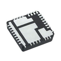
Pin Configuration
VIN
NC
ISET
NC
PVCC
PGND
PGND
PGND
ISL8204M, ISL8206M
(15 LD QFN)
TOP AND 3D VIEW
9
8
7
6
5
4
3
2
1 PGND
15 NC
PD1
14 FB
13 COMP/EN
PD4
PD2
PHASE 10
12 VOUT
PD3
11 PGND
Pin Descriptions
PIN
SYMBOL
DESCRIPTION
1, 2, 3, 4
PGND
Power ground pin for signal, input, and output return path. PGND needs to connect to one (or more) ground plane(s)
immediately, which is recommended to minimize the effect of switching noise, copper losses, and maximize heat
dissipation. Range: 0V.
5
PVCC
This pin provides the bias supply for ISL8204M, ISL8206M, as well as the low-side MOSFET’s gate and high-side
MOSFET’s gate. If PVCC rises above 6.5V, an internal 5V regulator will supply to the internal logics bias (but high-side
and low-side MOSFET gate will still be sourced by PVCC). Connect a well decoupled +5V or +12V supply to this pin.
Connect 1µF ceramic capacitor to ground plane directly. Range: 4.5V to 14.4V.
6, 8, 15
NC
No internal connection.
The ISET pin is the input for the overcurrent protection (OCP) setting, which compares the rDS(ON) of the low-side
MOSFET to set the overcurrent threshold. The ISL8204M, ISL8206M has an initial protect overcurrent limit. It has an
integrated internal 4.12k2.87k resistor (RSET-IN) between the ISET and PGND pins, which can prevent significant
overcurrent impact to the module. One can also connect an additional resistor RSET-EX between the ISET pin and the
PGND pin in order to reduce the current limit point by paralleling. Range: 0 to PVCC.
7
ISET
9
VIN
(PD1)
Power input pin. Apply input voltage between the VIN pin and PGND pin. It is recommended to place an input decoupling
capacitor directly between the VIN pin and the PGND pin. The input capacitor should be placed as closely as possible to
the module. Range: 1V to 20V.
10
PHASE
(PD2)
The PHASE pin is the switching node between the high and low-side MOSFET. It also returns the current path for the
high-side MOSFET driver and detects the low-side MOSFET drain voltage for the overcurrent limits point. Range: 0V to 30V.
11
PGND
(PD3)
Power ground pin for signal, input, and output return path. PGND needs to connect to one (or more) ground plane(s)
immediately, which is recommended to minimize the effect of switching noise, copper losses, and maximize heat
dissipation. Range: 0V.
12
VOUT
(PD4)
Power output pin. Apply output load between this pin and the PGND pin. It is recommended to place a high frequency
output decoupling capacitor directly between the VOUT pin and the PGND pin. The output capacitor should be placed as
closely as possible to the module. Range: 0.6V to 6V.
FN6999 Rev 4.00
October 28, 2014
Page 3 of 19
�ISL8204M, ISL8206M
Pin Descriptions
(Continued)
PIN
SYMBOL
DESCRIPTION
13
COMP/EN
This is the multiplexed pin of the ISL8204M, ISL8206M. During soft-start and normal converter operation, this pin
represents the output of the error amplifier. Use COMP/EN in combination with the FB pin to compensate for the voltage
control feedback loop of the converter. Pulling COMP/EN low (VENDIS = 0.4V nominal) will disable (shutdown) the controller,
which causes the oscillator to stop, and the high-side gate and low-side gate of the MOSFETs outputs to be held low. The
external pull-down device will initially need to overcome a maximum of 5mA of COMP/EN output current. However, once
the controller is disabled, the COMP/EN output will also be disabled, thus only a 20µA current source will continue to draw
current. Range: 0V to 5V.
14
FB
The FB pin is the output voltage adjustment of the ISL8204M, ISL8206M. It will regulate to 0.6V at the FB pin with
respect to the PGND pin. The ISL8204M, ISL8206M has an integrated voltage dividing resistor. This is a precision
9.76kΩ resistor (RFB-TI) between the VOUT and FB pins. Different output voltages can be programmed with
additional resistors between FB to PGND. Range: 0.6V.
FN6999 Rev 4.00
October 28, 2014
Page 4 of 19
�ISL8204M, ISL8206M
Absolute Maximum Ratings
Thermal Information
COMP/EN to PGND . . . . . . . . . . . . . . . . . . . . . . . . . . . . . . . . PGND - 0.3V to +6V
ISET to PGND . . . . . . . . . . . . . . . . . . . . . . . . . . . . . PGND - 0.3V to PVCC + 0.3V
PVCC to PGND . . . . . . . . . . . . . . . . . . . . . . . . . . . . . . . . . . PGND - 0.3V to +15V
PHASE to PGND (Note 4) . . . . . . . . . . . . . . . . . . . . . . . . . . . . . . . . -1.2V ~ +30V
VIN to PHASE (Note 4). . . . . . . . . . . . . . . . . . . . . . . . . . . . . . . . . . -1.2V ~ +30V
Junction Temperature, TJ . . . . . . . . . . . . . . . . . . . . . . . . . . . . . . . . . . +125°C
Storage Temperature Range, TSTG . . . . . . . . . . . . . . . . . . -55°C to +125°C
ESD Rating
Human Body Model (Tested per JESD22-A114E) . . . . . . . . . . . . . . . . 2kV
Machine Model (Tested per JESD22-A115-A) . . . . . . . . . . . . . . . . . 100V
Charge Device Model (Tested per JESD22-C101C). . . . . . . . . . . . . . . 1kV
Latch Up (Tested per JESD-78B; Class 2, Level A) . . . . . . . . . . . . . . 100mA
Thermal Resistance (Typical)
JA (°C/W) JC (°C/W)
15 Ld QFN (Notes 5, 6) . . . . . . . . . . . . . . . .
13.0
2.0
Pb-Free Reflow Profile . . . . . . . . . . . . . . . . . . . . . . . . . . . . . . . . . . see TB493
Recommended Operating Ratings
Input Supply Voltage (VIN) . . . . . . . . . . . . . . . . . . . . . . . . . . . . . +1V to +20V
Output Voltage (VOUT) . . . . . . . . . . . . . . . . . . . . . . . . . . . . . . . . . +0.6V to +6V
PVCC
Fixed Supply Voltage . . . . . . . . . . . . . . . . . . . . . . . . . . . . . . . +5V or +12V
Wide Range Supply . . . . . . . . . . . . . . . . . . . . . . . . . . . . . +6.5V to +14.4V
Ambient Temperature Range (TA) . . . . . . . . . . . . . . . . . . . -40°C to +85°C
CAUTION: Do not operate at or near the maximum ratings listed for extended periods of time. Exposure to such conditions may adversely impact product
reliability and result in failures not covered by warranty.
NOTES:
4. VDS (Drain to Source) specification for internal high-side and low-side MOSFET.
5. JA is measured in free air with the component mounted on a high effective thermal conductivity test board (i.e. 4-layer type without thermal vias
– see tech brief TB379) per JEDEC standards except that the top and bottom layers assume solid planes.
6. For JC, the “case temp” location is the center of the exposed metal pad on the package underside.
Electrical Specifications
TA = +25°C. VIN = 12V, VOUT = 1.5V. CIN = 220µFx1, 10µF/Ceramicx2, COUT = 47µFx8/Ceramic. Boldface limits
apply over the operating temperature range, -40°C to +85°C.
SYMBOL
CONDITIONS
MIN
(Note 8)
TYP
MAX
(Note 8)
UNITS
Input Supply Bias Current
IQ(VIN)
IOUT = 0A, VOUT = 1.5V, VIN = 12V, PVCC = 12V
-
13
-
mA
Input In-rush Current
IinRush
IOUT = 0A, VOUT = 1.5V, VIN = 12V, PVCC = 12V
-
140
-
mA
Input Supply Current
IS(VIN)
IOUT = 6A, VOUT = 1.5V, VIN = 12V, PVCC = 12V
-
0.86
-
A
IOUT = 4A, VOUT = 1.5V, VIN = 12V, PVCC = 12V
-
0.56
-
A
0
6
A
PARAMETER
INPUT CHARACTERISTICS
OUTPUT CHARACTERISTICS
Output Continuous Current Range
IOUT(DC)
VIN = 12V, VOUT = 1.5V
ISL8206M
ISL8204M
0
-
4
A
Line Regulation Accuracy
VOUT/VIN
VOUT = 1.5V, IOUT = 0A, VIN = 3.3V to 20V,
PVCC = 5V
-
0.1
-
%
Load Regulation Accuracy
VOUT/IOUT
IOUT = 0A to 6A/4A, VOUT = 1.5V, VIN = 12V,
PVCC = 12V
-
0.5
-
%
ISL8206M
-
8
-
mV
-
7
-
mV
Peak-to-Peak Output Ripple Voltage
VOUT
IOUT = 6A VOUT = 1.5V, VIN = 12V,
PVCC = 12V
ISL8204M
IOUT = 4A VOUT = 1.5V, VIN = 12V,
PVCC = 12V
DYNAMIC CHARACTERISTICS
Voltage Change For Positive Load Step
VOUT-DP
IOUT = 0A to 4A. Current slew rate = 2.5A/µs,
VIN = 12V, VOUT = 1.5V, PVCC = 12V
-
30
-
mV
Voltage Change For Negative Load Step
VOUT-DN
IOUT = 0A to 4A. Current slew rate = 2.5A/µs,
VIN = 12V, VOUT = 1.5V, PVCC = 12V
-
27
-
mV
FN6999 Rev 4.00
October 28, 2014
Page 5 of 19
�ISL8204M, ISL8206M
Electrical Specifications
TA = +25°C. VIN = 12V, VOUT = 1.5V. CIN = 220µFx1, 10µF/Ceramicx2, COUT = 47µFx8/Ceramic. Boldface limits
apply over the operating temperature range, -40°C to +85°C. (Continued)
PARAMETER
MIN
(Note 8)
TYP
MAX
(Note 8)
UNITS
IOUT = 0A to 6A. Current slew rate = 2.5A/µs,
VIN = 12V, VOUT = 1.5V, PVCC = 12V
-
43
-
mV
IOUT = 0A to 6A. Current slew rate = 2.5A/µs,
VIN = 12V, VOUT = 1.5V, PVCC = 12V
-
40
-
mV
PVCC = 12V; Disabled (Note 7)
4
5.2
7
mA
Fixed 5V supply (Note 7)
4.5
5.0
5.5
V
Wide range supply (Note 7)
6.5
12.0
14.4
V
5V supply
-
14
-
mA
12V supply
-
25
-
mA
-
14
-
mA
SYMBOL
CONDITIONS
Voltage Change For Positive Load Step
VOUT-DP
Voltage Change For Negative Load Step
VOUT-DN
CONTROLLER
PVCC Supply Current Shutdown
IPVCC_S
Supply Voltage
PVCC
PVCC Operating Current
IPVCC
IOUT = 6A, VOUT = 1.5V, VIN = 12V
IOUT = 4A, VOUT = 1.5V, VIN = 12V
5V supply
-
25
-
mA
Rising PVCC Threshold
VPORR
(Note 7)
12V supply
3.9
4.1
4.3
V
PVCC Power-On-Reset Threshold Hysteresis
VPORH
(Note 7)
0.30
0.35
0.40
V
Oscillator Frequency
FOSC
(Note 7)
510
600
660
kHz
Internal Resistor Between VOUT and FB Pins
RFB-TI
(Note 7)
9.66
9.76
9.86
k
Disabled Threshold Voltage (COMP/EN)
VENDIS
(Note 7)
0.375
0.4
0.425
V
Reference Voltage
VREF
Reference Voltage Tolerance
-
0.6
-
V
0°C to +70°C (Note 7)
(Note 7)
-1.0
-
+1.0
%
-40°C to +85°C (Note 7)
-1.5
-
+1.5
%
ISL8206M
-
4.12
-
k
ISL8204M
-
2.87
-
k
18.0
21.5
23.5
µA
FAULT PROTECTION
Internal Resistor Between ISET and PGND Pins
ISET Current Source
RSET-IN
ISET
(Note 7)
NOTES:
7. Parameters are 100% tested for internal IC/component prior to module assembly.
8. Parameters with MIN and/or MAX limits are 100% tested at +25°C, unless otherwise specified. Temperature limits established by characterization
and are not production tested.
FN6999 Rev 4.00
October 28, 2014
Page 6 of 19
�ISL8204M, ISL8206M
CPVCC
PVCC
VIN
(+5V/+12V)
VOUT
1.8V
10A
VIN
CIN (BULK)
220µF
VOUT
ISL8204M,
ISL8206M
PHASE
COMP/EN
CIN (CER)
10µF
25V
x2
COUT2
330µF
COUT1
22µF
6.3V
x3
FB
ISET
PGND
RFB
4.87k
FIGURE 4. TEST CIRCUIT FOR ALL PERFORMANCE AND DERATING GRAPHS
Typical Performance Characteristics
Efficiency Performance TA = +25°C, VIN = PVCC (PVCC = 5V for 18VIN), CIN = 220µFx1, 10µF/Ceramic x 2, COUT = 330µF (ESR = 10m),
22µF/Ceramic x 3. The efficiency equation is:
100
100
95
95
90
90
EFFICIENCY (%)
EFFICIENCY (%)
V OUT xI OUT
P OUT
Output Power
Efficiency = ----------------------------------------- = --------------- = ------------------------------------P IN
V IN xI IN
Input Power
85
80
3.3V
2.5V
75
1.5V
70
1.2V
65
60
1
2
3
5
4
80
75
3.3V
70
60
0
6
2.5V
1.5V
5.0V
65
0.8V
0
85
1
2
3
1.2V
4
0.8V
5
LOAD CURRENT (A)
LOAD CURRENT (A)
FIGURE 5. EFFICIENCY vs LOAD CURRENT (5VIN)
FIGURE 6. EFFICIENCY vs LOAD CURRENT (12VIN)
100
EFFICIENCY (%)
95
90
85
80
75
70
5.0V
2.5V
3.3V
1.5V
1.2V
65
60
0
1
2
3
4
5
6
LOAD CURRENT (A)
FIGURE 7. EFFICIENCY vs LOAD CURRENT (18VIN)
FN6999 Rev 4.00
October 28, 2014
Page 7 of 19
6
�ISL8204M, ISL8206M
Typical Performance Characteristics (Continued)
Transient Response Performance TA = +25°C, VIN = 12V, PVCC = 12V, CIN = 220µFx1, 10µF/Ceramic x 2, COUT = 330µF
(ESR = 10mΩ), 22µF/Ceramic x 3 IOUT = 0A to 5A, Current slew rate = 2.5A/µs
VOUT
VOUT
IOUT
VIN = 12V
VOUT = 1.2V
IOUT = 0A to 5A
IOUT
VIN = 12V
VOUT = 1.5V
IOUT = 0A to 5A
FIGURE 8. 1.2V TRANSIENT RESPONSE
FIGURE 9. 1.5V TRANSIENT RESPONSE
VOUT
VOUT
IOUT
VIN = 12V
VOUT = 1.8V
IOUT = 0A to 5A
IOUT
FIGURE 10. 1.8V TRANSIENT RESPONSE
VIN = 12V
VOUT = 2.5V
IOUT = 0A to 5A
FIGURE 11. 2.5V TRANSIENT RESPONSE
VOUT
IOUT
VIN = 12V
VOUT = 3.3V
IOUT = 0A to 5A
FIGURE 12. 3.3V TRANSIENT RESPONSE
FN6999 Rev 4.00
October 28, 2014
Page 8 of 19
�ISL8204M, ISL8206M
Typical Performance Characteristics (Continued)
Output Ripple Performance
Oscilloscope BW = 20MHz
TA = +25°C, VOUT = 1.5V, CIN = 220µFx1, 10µF/Ceramic x 2, COUT = 47µF/Ceramic x 8.
VOUT 6A
VOUT 6A
VOUT 4A
VOUT 4A
VOUT 0A
VOUT 0A
FIGURE 13. OUTPUT VOLTAGE RIPPLE AT VIN = 5V
FIGURE 14. OUTPUT VOLTAGE RIPPLE AT VIN = 12V
Reference Circuitry For General
Applications
1. Single Power Supply
2. Separated Power Supply
Figure 16 shows the ISL8204M, ISL8206M application
schematic for wide input voltages from +1V to +20V. The
PVCC supply can source +5V/+12V or +6.5V to 14.4V.
Figure 15 shows the ISL8204M, ISL8206M application
schematic for input voltage +5V or +12V. The PVCC pin can
connect to the input supply directly.
(+5V/+12V)
P VCC
or
(+6.5V to 14.4V) C PVCC
C PVCC
PVCC
(+1V to +20V)
CO M P/EN
PVCC
COMP/EN
VIN
ISL8204M, ISL8206M
FB
PHASE
R FB
R SET-EX
ISET
PGND
VIN
V IN
C IN
ISL8204M , ISL8206M
FB
PHASE
(+5V/+12V)
V IN
C IN
R FB
R SET-EX
ISET
PG ND
V OUT
VO UT
C OUT
V OUT
VOUT
C OUT
FIGURE 15. TYPICAL APPLICATION SCHEMATIC
FIGURE 16. WIDE INPUT VOLTAGE APPLICATION SCHEMATIC
Applications Information
The typical ISL8204M, ISL8206M application schematic for input
voltage +5V or +12V is shown in Figure 15. External component
selection is primarily determined by the maximum load current
and input/output voltage.
Programming the Output Voltage
The ISL8204M, ISL8206M has an internal 0.6V ±1.5% reference
voltage. Programming the output voltage requires a dividing
resistor (RFB). The output voltage can be calculated as shown in
Equation 1:
9.76k
V OUT = 0.6 1 + ---------------
R
FB
FN6999 Rev 4.00
October 28, 2014
(EQ. 1)
Page 9 of 19
�ISL8204M, ISL8206M
Note: ISL8204M, ISL8206M has integrated 9.76k resistance into
the module (dividing resistor for top side). The resistance
corresponding to different output voltages is as shown in Table 2:
TABLE 2. RESISTANCE TO OUTPUT VOLTAGES
VOUT
0.6V
0.8V
1.05V
1.2V
RFB
open
28.7k
13k
9.76k
VOUT
1.5V
1.8V
2.5V
3.3V
RFB
6.49k
4.87k
3.09k
2.16k
VOUT
5V
6V
RFB
1.33k
1.07k
bias regulator can turn on cleanly. At the same time, the ISET pin
is initialized by disabling the low-side gate driver and drawing ISET
(nominal 21.5µA) through RSETI. This sets up a voltage that will
represent the ISET trip point. At t2, there is a variable time period
for the OCP sample and hold operation (0.0ms to 3.4ms
nominal; the longer time occurs with the higher overcurrent
setting). The sample and hold operation uses a digital counter
and DAC to save the voltage, so the stored value does not
degrade, as long as the PVCC is above VPORR (see “Overcurrent
Protection (OCP)” on page 12 for more details on the equations
and variables). Upon the completion of sample and hold at T3,
the soft-start operation is initiated, and the output voltage ramps
up between t4 and t5.
COMP/EN
COMP/EN
Initialization (POR and OCP Sampling)
Figure 17 shows a start-up waveform of ISL8204M, ISL8206M.
The power-on-reset (POR) function continually monitors the bias
voltage at the PVCC pin. Once the rising POR threshold has
exceeded 4V (VPORR nominal), the POR function initiates the
overcurrent protection (OCP) sample and hold operation (while
COMP/EN is ~1V). When the sampling is complete, VOUT begins
the soft-start ramp.
Tt00
Tt11
ISET
ISET
VOUT
VOUT
PVCC
FIGURE 18. ISET AND SOFT-START OPERATION
VOUT
~4V
START SWITCHING
COMP/EN
t1
t2
t3
t5
t4
COMP/EN
FIGURE 17. POR AND SOFT-START OPERATION
ISET
If the COMP/EN pin is held low during power-up, the initialization
will be delayed until the COMP/EN is released and its voltage
rises above the VENDIS trip point.
VOUT
Figures 18 and 19 show a typical power-up sequence in more
detail. The initialization starts at t0, when either PVCC rises above
VPORR, or the COMP/EN pin is released (after POR). The
COMP/EN will be pulled up by an internal 20µA current source,
however, the timing will not begin until the COMP/EN exceeds
the VENDIS trip point (at t1). The external capacitance of the
disabling device, as well as the compensation capacitors, will
determine how quickly the 20µA current source will charge the
COMP/EN pin. With typical values, it should add a small delay
compared to the soft-start times. The COMP/EN will continue to
ramp to ~1V.
From t1, there is a nominal 6.8ms delay, which allows the PVCC
pin to exceed 6.5V (if rising up towards 12V), so that the internal
FN6999 Rev 4.00
October 28, 2014
3.4ms
3.4ms
FIGURE 19. ISET AND SOFT-START OPERATION
Soft-Start and Pre-Biased Outputs
The soft-start internally ramps the reference on the non-inverting
terminal of the error amp from 0V to 0.6V in a nominal 6.8ms.
The output voltage will follow the ramp from zero to its final value
in the same 6.8ms (the actual ramp seen on VOUT will be less
than the nominal time), due to some initialization timing
between t3 and t4.
Page 10 of 19
�ISL8204M, ISL8206M
The ramp is created digitally, so there will be 64 small discrete
steps. There is no simple way to change this ramp rate externally.
After an initialization period (t3 to t4), the error amplifier (COMP/EN
pin) is enabled and begins to regulate the converter's output voltage
during soft-start. The oscillator's triangular waveform is compared to
the ramping error amplifier voltage. This generates PHASE pulses of
increasing width that charge the output capacitors. When the
internally generated soft-start voltage exceeds the reference voltage
(0.6V), the soft-start is complete and the output should be in
regulation at the expected voltage. This method provides a rapid and
controlled output voltage rise; there is no large in-rush current
charging the output capacitors. The entire start-up sequence from
POR typically takes up to 17ms; up to 10.2ms for the delay and OCP
sample and 6.8ms for the soft-start ramp.
VOUT
Figure 20 shows the normal curve for start-up; initialization
begins at t0, and the output ramps between t1 and t2. If the
output is pre-biased to a voltage less than the expected value (as
shown Figure 21), neither internal MOSFET will turn on until the
soft-start ramp voltage exceeds the output; VOUT starts
seamlessly ramping from there.
FIGURE 21. PRE-BIASED START-UP
VOUT
VOUT
T2
T1
T0
FIGURE 20. NORMAL START-UP
If the output is pre-biased to a voltage above the expected value
(as shown Figure 22), neither MOSFET will turn on until the end of
the soft-start, at which time it will pull the output voltage down to
the final value. Any resistive load connected to the output will help
pull down the voltage (at the RC rate of the R of the load and the C
of the output capacitance).
500mV/DIV
FIGURE 22. PRE-BIASED START-UP - OVERCHARGED
If VIN for the synchronous buck converter is from a different
supply that comes up after PVCC, the soft-start will go through its
cycle, but with no output voltage ramp. When VIN turns on, the
output will follow the ramp of the VIN from zero up to the final
expected voltage (at close to 100% duty cycle, with COMP/EN pin
>4V). If VIN is too fast, there may be excessive in-rush current
charging the output capacitors (only the beginning of the ramp,
from zero to VOUT matters here). If this is not acceptable, then
consider changing the sequencing of the power supplies, sharing
the same supply, or adding sequencing logic to the COMP/EN pin
to delay the soft-start until the VIN supply is ready (see “Input
Voltage Considerations” on page 13).
If ISL8204M, ISL8206M is disabled after soft-start (by pulling
COMP/EN pin low), and afterwards enabled (by releasing the
COMP/EN pin), then the full initialization (including OCP sample)
will take place. However, there is no new OCP sampling during
FN6999 Rev 4.00
October 28, 2014
Page 11 of 19
�ISL8204M, ISL8206M
overcurrent retries. If the output is shorted to GND during
soft-start, the OCP will handle it, as described in the next section.
Overcurrent Protection (OCP)
The overcurrent function protects the converter from a shorted
output by using the low-side MOSFET ON-resistance, rDS(ON), to
monitor the current. A resistor (RSET) programs the overcurrent
trip level.
This method enhances the converter's efficiency and reduces
cost by eliminating a current sensing resistor. If overcurrent is
detected, the output immediately shuts off. It cycles the soft-start
function in a hiccup mode (2 dummy soft-start time-outs, then up
to one real one) to provide fault protection. If the shorted
condition is not removed, this cycle will continue indefinitely.
Following POR (and 6.8ms delay), the ISL8204M, ISL8206M
initiates the overcurrent protection sample and hold operation.
The low-side gate driver is disabled to allow an internal 21.5µA
current source to develop a voltage across RSET. The ISL8204M,
ISL8206M samples this voltage (which is referenced to the PGND
pin) at the ISET pin, and holds it in a counter and DAC
combination. This sampled voltage is held internally as the
overcurrent set point, for as long as power is applied, or until a
new sample is taken after coming out of a shutdown.
The actual monitoring of the low-side MOSFET ON-resistance
starts 200ns (nominal) after the edge of the internal PWM logic
signal (that creates the rising external low-side gate signal). This
is done to allow the gate transition noise and ringing on the
PHASE pin to settle out before monitoring. The monitoring ends
when the internal PWM edge (and thus low-side gate signal) goes
low. The OCP can be detected anywhere within the above
window.
If the converter is running at high duty cycles, around 75% for
600kHz operation, then the low-side gate pulse width may not be
wide enough for the OCP to properly sample the rDS(ON). For those
cases, if the low-side gate signal is too narrow (or not there at all)
for 3 consecutive pulses, then the third pulse will be stretched
and/or inserted to the 425ns minimum width. This allows for
OCP monitoring every third pulse under this condition. This can
introduce a small pulse-width error on the output voltage, which
will be corrected on the next pulse; and the output ripple voltage
will have an unusual 3-clock pattern, which may look like jitter.
The overcurrent function will trip at a peak inductor current
(IPEAK) determined by Equation 2:
2 I SET R SET
I PEAK = -------------------------------------------r DS ON
(EQ. 2)
where:
ISET is the internal ISET current source (21.5µA typical).
RSET is equivalent resistance between ISET and PGND pins.
rDS(ON) is typically 15m at (VPVCC = VGS = 10V, IDS = 15A) and
18m at (VPVCC = VGS = 4.5V, IDS = 15A).
FN6999 Rev 4.00
October 28, 2014
Note: ISL8204M, ISL8206M has integrated 4.12k2.87k
resistance (RSET-IN). Therefore, the equivalent resistance of RSET
can be expressed in Equation 3:
R SET-EX R SET-IN
R SET = ------------------------------------------------------R SET-EX + R SET-IN
(EQ. 3)
The scale factor of 2 doubles the trip point of the MOSFET voltage
drop, compared to the setting on the RSET resistor. The OC trip
point varies in a system mainly due to the MOSFET rDS(ON)
variations (i.e. over process, current and temperature). To avoid
overcurrent tripping in the normal operating load range, find the
RSET resistor from Equation 3, and use the following values:
1. The maximum rDS(ON) at the highest junction temperature
2. The minimum ISET from the “Electrical Specifications” table
on page 3.
3. Determine IPEAK for:
I L
I PEAK I OUT MAX + ------------2
(EQ. 4)
where IL is the output inductor ripple current. In a high input
voltage, high output voltage application, such as 20V input to 5V
output, the inductor ripple becomes excessive due to the fix
internal inductor value. In such applications, the output current will
be limited from the rating to approximately 70% of the module’s
rated current.
The relationships between the external RSET values and the
typical output current IOUT(MAX) OCP levels for ISL8206M are as
follows:
TABLE 3.
RSET
()
OCP (A) at
VIN = 12V,
PVCC = 5V
OCP (A) at
VIN = 12V
PVCC = 12V
OPEN
8.1
8.8
50k
7.5
8.1
20k
6.6
7.4
10k
5.5
6.4
5k
4.4
5.0
The range of allowable voltages detected (2 x ISET x RSET) is 0mV to
475mV. If the voltage drop across RSET is set too low, the following
conditions may occur: (1) Continuous OCP tripping and retry and
(2) It may be overly sensitive to system noise and in-rush current
spikes, so it should be avoided. The maximum usable setting is
around 0.2V across RSET (0.4V across the MOSFET); values above
this might disable the protection. Any voltage drop across RSET
that is greater than 0.3V (0.6V MOSFET trip point) will disable the
OCP. Note that conditions during power-up or during a retry may
look different than normal operation. During power-up in a 12V
system, the ISL8204M, ISL8206M starts operation just above 4V;
if the supply ramp is slow, the soft-start ramp might be over well
before 12V is reached. Therefore, with low-side gate drive voltages,
the rDS(ON) of the MOSFET will be higher during power-up,
effectively lowering the OCP trip. In addition, the ripple current will
likely be different at a lower input voltage. Another factor is the
digital nature of the soft-start ramp. On each discrete voltage step,
there is in effect, a small load transient and a current spike to
charge the output capacitors. The height of the current spike is not
Page 12 of 19
�ISL8204M, ISL8206M
controlled, however, it is affected by the step size of the output and
the value of the output capacitors, as well as the internal error
amp compensation. Therefore, it is possible to trip the overcurrent
with in-rush current, in addition to the normal load and ripple
considerations.
Figure 23 shows the output response during a retry of an output
shorted to PGND. At time t0, the output has been turned off due to
sensing an overcurrent condition. There are two internal soft-start
delay cycles (t1 and t2) to allow the MOSFETs to cool down in order
to keep the average power dissipation in retry at an acceptable
level. At time t2, the output starts a normal soft-start cycle, and the
output tries to ramp. If the short is still applied and the current
reaches the ISET trip point any time during the soft-start ramp
period, the output will shut off and return to time t0 for another
delay cycle. The retry period is thus two dummy soft-start cycles
plus one variable (which depends on how long it takes to trip the
sensor each time). Figure 23 shows an example where the output
gets about half-way up before shutting down; therefore, the retry
(or hiccup) time will be around 17ms. The minimum should be
nominally 13.6ms and the maximum 20.4ms. If the short
condition is finally removed, the output should ramp up normally
on the next t2 cycle.
typical power supply to ramp up past 6.5V before the soft-start
ramps begins. This prevents a disturbance on the output, due to
the internal regulator turning on or off. If the transition is slow (not
a step change), the disturbance should be minimal. Thus, while the
recommendation is to not have the output enabled during the
transition through this region, it may be acceptable. The user
should monitor the output for their application to see if there is any
problem. If PVCC powers up first and VIN is not present by the time
the initialization is done, then the soft-start will not be able to
ramp the output, and the output will later follow part of the VIN
ramp when it is applied. If this is not desired, then change the
sequencing of the supplies, or use the COMP/EN pin to disable
VOUT until both supplies are ready.
Figure 24 shows a simple sequencer for this situation. If PVCC
powers up first, Q1 will be off, and R3 pulling to PVCC will turn Q2
on, keeping the ISL8204M, ISL8206M in shutdown. When VIN
turns on, the resistor divider R1 and R2 determine when Q1 turns
on, which will turn off Q2 and release the shutdown. If VIN powers
up first, Q1 will be on, turning Q2 off; so the ISL8204M,
ISL8206M will start up as soon as PVCC comes up. The VENDIS trip
point is 0.4V nominal, so a wide variety of N-MOSFET or NPN BJT
or even some logic IC's can be used as Q1 or Q2. However, Q2
must be low leakage when off (open-drain or open-collector) so
as not to interfere with the COMP output. Q2 should also be
placed near the COMP/EN pin.
VIN
T0
T1
~6.8ms
PVCC
R3
T2
R1
TO COMP/EN
~6.8ms
R2
VOUT
Q1
Q2
FIGURE 24. SEQUENCE CIRCUIT
FIGURE 23. OVERCURRENT RETRY OPERATION
Starting up into a shorted load looks the same as a retry into that
same shorted load. In both cases, OCP is always enabled during
soft-start; once it trips, it will go into retry (hiccup) mode. The
retry cycle will always have two dummy time-outs, plus whatever
fraction of the real soft-start time passes before the detection
and shutoff. At that point, the logic immediately starts a new two
dummy cycle time-out.
Input Voltage Considerations
Figure 16 shows a standard configuration where PVCC is either 5V
(±10%) or 12V (±20%). In each case, the gate drivers use the
PVCC voltage for low-side gate and high-side gate driver. In
addition, PVCC is allowed to work anywhere from 6.5V up to the
14.4V maximum. The PVCC range between 5.5V and 6.5V is not
allowed for long-term reliability reasons, but transitions through
it to voltages above 6.5V are acceptable.
There is an internal 5V regulator for bias, which turns on between
5.5V and 6.5V. Some of the delay after POR is there to allow a
FN6999 Rev 4.00
October 28, 2014
The VIN range can be as low as ~1V (for VOUT as low as the 0.6V
reference) and as high as 20V. There are some restrictions for
running high VIN voltage. The maximum PHASE voltage is 30V.
VIN + PVCC + any ringing or other transients on the PHASE pin
must be less than 30V. If VIN is 20V, it is recommended to limit
PVCC to 5V.
Switching Frequency
The switching frequency is a fixed 600kHz clock, which is
determined by the internal oscillator. However, all of the other
timing mentioned (POR delay, OCP sample, soft-start, etc.) is
independent of the clock frequency (unless otherwise noted).
Selection of the Input Capacitor
The input filter capacitor should be based on how much ripple
the supply can tolerate on the DC input line. The larger the
capacitor, the less ripple expected but consideration should be
taken for the higher surge current during power-up. The
ISL8204M, ISL8206M provides the soft-start function that
Page 13 of 19
�ISL8204M, ISL8206M
controls and limits the current surge. The value of the input
capacitor can be calculated by Equation 5:
• The ground connection between pin 11 and pins 1 through 4
should be a solid ground plane under the module.
I IN t
C IN = ------------------V
• Place a high frequency ceramic capacitor between (1) VIN and
PGND (pin 11) and (2) PVCC and PGND (pins 1 through 4) as
close to the module as possible to minimize high frequency
noise.
(EQ. 5)
Where:
CIN is the input capacitance (µF)
• Use large copper areas for a power path (VIN, PGND, VOUT) to
minimize conduction loss and thermal stress. Also, use
multiple vias to connect the power planes in different layers.
IIN is the input current (A)
t is the turn on time of the high-side switch (µs)
• Keep the trace connection to the feedback resistor short.
V is the allowable peak-to-peak voltage (V)
• Avoid routing any sensitive signal traces near the PHASE node.
In addition to the bulk capacitance, some low Equivalent Series
Inductance (ESL) ceramic capacitance is recommended to
decouple between the drain terminal of the high-side MOSFET
and the source terminal of the low-side MOSFET. This is used to
reduce the voltage ringing created by the switching current
across parasitic circuit elements.
CPVCC
PGND
VIN
RFB
Output Capacitors
The ISL8204M, ISL8206M is designed for low output voltage
ripple. The output voltage ripple and transient requirements can
be met with bulk output capacitors (COUT) with low enough
Equivalent Series Resistance (ESR). COUT can be a low ESR
tantalum capacitor, a low ESR polymer capacitor or a ceramic
capacitor. The typical capacitance is 330µF and decoupled
ceramic output capacitors are used. The internally optimized
loop compensation provides sufficient stability margins for all
ceramic capacitor applications with a recommended total value
of 400µF. Additional output filtering may be needed if further
reduction of output ripple or dynamic transient spike is required.
VOUT
CIN
COUT1
(DECOUPLE)
PGND
FIGURE 25. RECOMMENDED LAYOUT
Layout Guide
To achieve stable operation, low losses and good thermal
performance some layout considerations are necessary.
7
3.0
6
LOSS (W)
2.5
MAX LOAD CURRENT (A)
3.5
3.3V
1.5V
2.0
0.6V
1.5
1.0
0.5
0.0
0
1
2
3
4
5
LOAD CURRENT (A)
FIGURE 26. POWER LOSS vs LOAD CURRENT (5VIN)
FN6999 Rev 4.00
October 28, 2014
6
5
3.3V
1.5V
4
0.6V
3
2
1
0
60
70
80
90
100
110
AMBIENT TEMPERATURE (°C)
FIGURE 27. DERATING CURVE (5VIN)
Page 14 of 19
�ISL8204M, ISL8206M
4.0
7
3.3V
3.0
LOSS (W)
MAX LOAD CURRENT (A)
5.0V
3.5
2.5
2.5V
1.5V
0.6V
2.0
1.5
1.0
0.5
0.0
0
1
2
3
4
5
6
6
5
5.0V
4
Thermal Considerations
Experimental power loss curves along with JA from thermal
modeling analysis can be used to evaluate the thermal
consideration for the module. The derating curves are derived
from the maximum power allowed while maintaining the
temperature below the maximum junction temperature of
+125°C. The power loss and derating curves apply for both
ISL8206M, and ISL8204M. The loss at 4A can be found by
tracing the power loss curve up at the load current of 4A. In
actual applications, other heat sources and design margins
should be considered.
Package Description
The structure of ISL8204M, ISL8206M belongs to the Quad
Flat-pack No-lead package (QFN). This kind of package has
advantages, such as good thermal and electrical conductivity, low
weight and small size. The QFN package is applicable for surface
mounting technology and is being more readily used in the
industry. The ISL8204M, ISL8206M contains several types of
devices, including resistors, capacitors, inductors and control ICs.
The ISL8204M, ISL8206M is a copper lead-frame based package
with exposed copper thermal pads, which have good electrical and
thermal conductivity. The copper lead frame and multi-component
assembly is overmolded with polymer mold compound to protect
these devices.
The package outline and typical PCB layout pattern design and
typical stencil pattern design are shown in the package outline
drawing L15.15x15 on page 18. The module has a small size of
15mmx15mmx3.5mm. Figure 30 shows typical reflow profile
parameters. These guidelines are general design rules. Users can
modify parameters according to their application.
PCB Layout Pattern Design
The bottom of ISL8204M, ISL8206M is a lead-frame footprint,
which is attached to the PCB using a surface mounting process.
The PCB layout pattern is shown in the Package Outline Drawing
L15.15x15 on page 18. The PCB layout pattern is essentially 1:1
with the QFN exposed pad and I/O termination dimensions,
except for the PCB lands being a slightly extended distance of
0.2mm (0.4mm max) longer than the QFN terminations, which
allows for solder filleting around the periphery of the package.
This ensures a more complete and inspectable solder joint. The
FN6999 Rev 4.00
October 28, 2014
2.5V
3
1.5V
0.6V
2
1
0
60
70
LOAD CURRENT (A)
FIGURE 28. POWER LOSS vs LOAD CURRENT (12VIN)
3.3V
80
90
100
110
AMBIENT TEMPERATURE (°C)
FIGURE 29. DERATING CURVE (12VIN)
thermal lands on the PCB layout should match 1:1 with the
package exposed die pads.
Thermal Vias
A grid of 1.0mm to 1.2mm pitch thermal vias, which drops down
and connects to buried copper plane(s), should be placed under
the thermal land. The vias should be about 0.3mm to 0.33mm in
diameter with the barrel plated to about 1.0 ounce copper.
Although adding more vias (by decreasing via pitch) will improve
the thermal performance, diminishing returns will be seen as
more and more vias are added. Simply use as many vias as
practical for the thermal land size and your board design rules
allow.
Stencil Pattern Design
Reflowed solder joints on the perimeter I/O lands should have
about a 50µm to 75µm (2mil to 3mil) standoff height. The solder
paste stencil design is the first step in developing optimized,
reliable solder joints. Stencil aperture size to land size ratio
should typically be 1:1. The aperture width may be reduced
slightly to help prevent solder bridging between adjacent I/O
lands. To reduce solder paste volume on the larger thermal
lands, it is recommended that an array of smaller apertures be
used instead of one large aperture. It is recommended that the
stencil printing area cover 50% to 80% of the PCB layout pattern.
A typical solder stencil pattern is shown in the Package Outline
Drawing L15.15x15 on page 18. The gap width between pad to
pad is 0.6mm. The user should consider the symmetry of the
whole stencil pattern when designing its pads. A laser cut,
stainless steel stencil with electropolished trapezoidal walls is
recommended. Electropolishing “smooths” the aperture walls
resulting in reduced surface friction and better paste release
which reduces voids. Using a trapezoidal section aperture (TSA)
also promotes paste release and forms a "brick like" paste
deposit that assists in firm component placement. A 0.1mm to
0.15mm stencil thickness is recommended for this large pitch
(1.3mm) QFN.
Page 15 of 19
�ISL8204M, ISL8206M
Reflow Parameters
300
PEAK TEMPERATURE +230°C~+245°C;
TYPICALLY 60s-70s ABOVE +220°C
KEEP LESS THAN 30s WITHIN 5°C OF PEAK TEMP.
250
TEMPERATURE (°C)
Due to the low mount height of the QFN, "No Clean" Type 3 solder
paste per ANSI/J-STD-005 is recommended. Nitrogen purge is
also recommended during reflow. A system board reflow profile
depends on the thermal mass of the entire populated board, so it
is not practical to define a specific soldering profile just for the
QFN. The profile given in Figure 30 is provided as a guideline, to
be customized for varying manufacturing practices and
applications.
200 SLOW RAMP (3°C/s MAX)
AND SOAK FROM +100°C
TO +180°C FOR 90s~120s
150
100
RAMP RATE 1.5°C FROM +70°C TO +90°C
50
0
0
100
150
200
250
300
350
DURATION (s)
FIGURE 30. TYPICAL REFLOW PROFILE
Revision History
The revision history provided is for informational purposes only and is believed to be accurate, but not warranted.
Please go to web to make sure you have the latest Rev.
DATE
REVISION
CHANGE
October 28, 2014
FN6999.4
Updated Storage Temperature Range, TSTG page 5 from “-40°C to +155°C” to “-55°C to +155°C”.
Replaced Note 2 with the following: “These Intersil plastic packaged products are RoHS compliant by EU
exemption 7C-I and employ special Pb-free material sets, molding compounds/die attach materials, and 100%
matte tin plate plus anneal (e3) termination finish which is compatible with both SnPb and Pb-free soldering
operations. Intersil RoHS compliant products are MSL classified at Pb-free peak reflow temperatures that meet
or exceed the Pb-free requirements of IPC/JEDEC J STD-020.”
Updated Products verbiage to About Intersil verbiage on page 17.
June 19, 2012
FN6999.3
On page 9:
Changed conditions for Output Ripple Performance waveforms on from:
TA = +25C, VIN = 12V, PVCC = 12V, CIN = 220µFx1, 10µF/Ceramic x 2, COUT = 330µF (ESR = 10mΩ),
22µF/Ceramic x 3 IOUT = 0, 4, 6A
To:
TA = +25C, VOUT = 1.5V, CIN = 220µFx1, 10µF/Ceramic x 2, COUT = 47µF/Ceramic x 8
Removed 2.5V OUTPUT RIPPLE and 3.3V OUTPUT RIPPLE waveforms
Replaced Figures 13 and 14. Changed Figure 13 caption from “1.2V OUTPUT RIPPLE” to “OUTPUT VOLTAGE
RIPPLE AT VIN = 5V”. Changed Figure 14 caption from “1.5V OUTPUT RIPPLE” to “OUTPUT VOLTAGE RIPPLE AT
VIN = 12V”
© Copyright Intersil Americas LLC 2009-2014. All Rights Reserved.
All trademarks and registered trademarks are the property of their respective owners.
For additional products, see www.intersil.com/en/products.html
Intersil products are manufactured, assembled and tested utilizing ISO9001 quality systems as noted
in the quality certifications found at www.intersil.com/en/support/qualandreliability.html
Intersil products are sold by description only. Intersil may modify the circuit design and/or specifications of products at any time without notice, provided that such
modification does not, in Intersil's sole judgment, affect the form, fit or function of the product. Accordingly, the reader is cautioned to verify that datasheets are
current before placing orders. Information furnished by Intersil is believed to be accurate and reliable. However, no responsibility is assumed by Intersil or its
subsidiaries for its use; nor for any infringements of patents or other rights of third parties which may result from its use. No license is granted by implication or
otherwise under any patent or patent rights of Intersil or its subsidiaries.
For information regarding Intersil Corporation and its products, see www.intersil.com
FN6999 Rev 4.00
October 28, 2014
Page 16 of 19
�ISL8204M, ISL8206M
Revision History
The revision history provided is for informational purposes only and is believed to be accurate, but not warranted.
Please go to web to make sure you have the latest Rev. (Continued)
DATE
REVISION
CHANGE
October 13, 2010
FN6999.2
Updated the Simplified Block Diagram Figure 3 on page 2. Difference is on the ground connection near RSET-IN.
Page 17 under Reflow Parameters corrected number from “ANSI/J-STD-00” to “ANSI/J-STD-005”.
Changed Note 2 in ordering information from “These products do contain Pb but they are RoHS compliant by EU
exemption 5 (Pb in glass of cathode ray tubes, electronic
components and fluorescent tubes”. To “These Intersil plastic packaged products employ special material sets,
molding compounds and 100% matte tin plate plus anneal (e3) termination finish. These products do contain
Pb but they are RoHS compliant by EU exemption 5 (Pb in glass of cathode ray tubes, electronic components
and fluorescent tubes ). These Intersil RoHS compliant products are compatible with both SnPb and Pb-free
soldering operations. These Intersil RoHS compliant products are MSL classified at Pb-free peak reflow
temperatures that meet or exceed the Pb-free requirements of IPC/JEDEC J STD-020.
On page 1:
Replaced Note 2 with the following: “These products do contain Pb but they are RoHS compliant by EU
exemption 5 (Pb in glass of cathode ray tubes, electronic components and fluorescent tubes).“
On page 4:
-Added Theta JC bottom : 2.0 C/W
-Changed Note 5: Theta-JA is measured in free air with the component mounted on a high effective thermal
conductivity test board (i.e. 4-layer type without thermal vias – see tech brief TB379) per JEDEC standards
except that the top and bottom layers assume solid planes.
-Added note: For Theta-JC bottom, the “case temp” location is the center of the package underside.
Updated Package Outline Drawing page 18:
Corrected pad width dimension in land pattern on page 19 from 3.10 to 3.00
(7th line down from top in column on left handside)
-Changes to Figure 30 as follows: From: “ SLOW RAMP AND SOAK …” To: “ SLOW RAMP (3C/sec max) AND SOAK
… “ From: “PEAK TEMPERATURE =230 – 245C; KEEP ABOUT 30s ABOVE 220 “
To: “PEAK TEMPERATURE = 230-245C ; typically 60s-70s ABOVE 220. Keep less than 30s within 5 degrees of
peak temp
-Changed the graphic to look more like 65 sec above 220 and 25 sec within 5 C of peak.
-Updated POD to most recent version -Added dimension 15.8+/-0.2 to bottom and right side of TOP VIEW.
changed 0.4+/-0.2 to (33x0.4)
Added Eval boards to ordering information
February 25, 2010
FN6999.1
Updated title. Replaced Figures 3 and 7.
December 21, 2009
FN6999.0
Initial Release.
About Intersil
Intersil Corporation is a leading provider of innovative power management and precision analog solutions. The company's products
address some of the largest markets within the industrial and infrastructure, mobile computing and high-end consumer markets.
For the most updated datasheet, application notes, related documentation and related parts, please see the respective product
information page found at www.intersil.com.
You may report errors or suggestions for improving this datasheet by visiting www.intersil.com/ask.
Reliability reports are also available from our website at www.intersil.com/support
FN6999 Rev 4.00
October 28, 2014
Page 17 of 19
�ISL8204M, ISL8206M
FN6999 Rev 4.00
October 28, 2014
Package Outline Drawing
L15.15x15
15 LEAD QUAD FLAT NO-LEAD PLASTIC PACKAGE (PUNCH QFN)
Rev 3, 8/10
23X 1.30
2X 7.70
7x 1.70
4X 1.90
1.80
5.90
PIN 1
INDEX AREA
1 1514 13
X4
12
2
3
4
5
6
7
8
1.30
0.2 S AB
12
13 14 15 1
2
3
4
5
6
7
8
3.80
3.10
11
15.0±0.2 15.8±0.2
11
2.10
13.80
9.0
5.0
9
10
(33x0.4)
15.0±0.2
2.10
0.30
6.90
6.0000
2.90
2X 1.125
5.80
21X 1.0
15.8±0.2
0.90
5.10
1.90
45°
10
0.05 M S AB 33x 0.5
9
11X 0.80
3.0
4.80
4.60
2.20
TOP VIEW
4X 7.90
BOTTOM VIEW
5° ALL AROUND
0.2 S
3.5±0.2
0.5
0.05 S
S
SIDE VIEW
NOTES:
Page 18 of 19
1.
Dimensions are in millimeters.
2.
Unless otherwise specified, tolerance : Decimal ± 0.05;
Body Tolerance ±0.1mm
3.
The configuration of the pin #1 identifier is optional, but must be
located within the zone indicated. The pin #1 indentifier may be
either a mold or mark feature.
�4.12
3.48
2.82
2.18
1.52
0.88
2.38
0.42
0.00
0.22
4.98
4.32
3.68
3.02
8.30
6.92
6.28
5.62
8.30
5.60
4.60
1.30
2.30
3.10
3.60
4.40
4.90
5.70
6.20
7.00
8.29
6.18
5.60
4.80
4.30
3.50
3.00
Package Boundary
2.20
8.30
1.70
6.00
0.90
5.10
0.40
0.0
3.10
0.0
0.40
2.10
0.90
6.08
8.29
5.52
6.99
5.52
4.22
4.87
4.22
3.57
2.92
2.27
1.62
0.97
0.32
0.00
0.33
3.58
2.92
2.28
1.62
0.98
0.32
0.00
0.32
0.98
1.63
2.28
2.93
3.58
4.23
0.98
1.70
2.20
0.90
1.90
1.63
2.28
3.00
4.00
8.30
2.93
4.88
8.30
5.53
4.88
5.53
7.01
8.30
6.60
5.90
4.30
2.18
0.00
1.35
1.00
1.60
2.80
4.90
STENCIL PATTERN WITH SQUARE PADS-2
6.60
6.60
4.80
3.75
3.40
3.15
1.80
0.30
0.00
0.00
0.60
0.30
3.15
1.20
3.60
3.75
3.70
4.30
2.00
1.40
0.00
0.90
2.50
6.60
4.30
4.20
6.60
4.90
4.30
6.70
Page 19 of 19
2.20
STENCIL PATTERN WITH SQUARE PADS-1
8.30
6.72
7.00
1.52
2.18
2.82
3.48
4.12
6.07
0.22
0.88
0.42
0.00
3.02
2.38
3.50
5.27
4.63
4.15
TYPICAL RECOMMENDED LAND PATTERN
7.00
8.31
8.30
5.60
4.60
0.0
1.20
2.20
3.10
5.20
8.30
1
ISL8204M, ISL8206M
FN6999 Rev 4.00
October 28, 2014
8.30
6.10
�


 工商网监
湘ICP备2023018690号
工商网监
湘ICP备2023018690号
