Silicon N-Channel
Power MOSFET
R
○
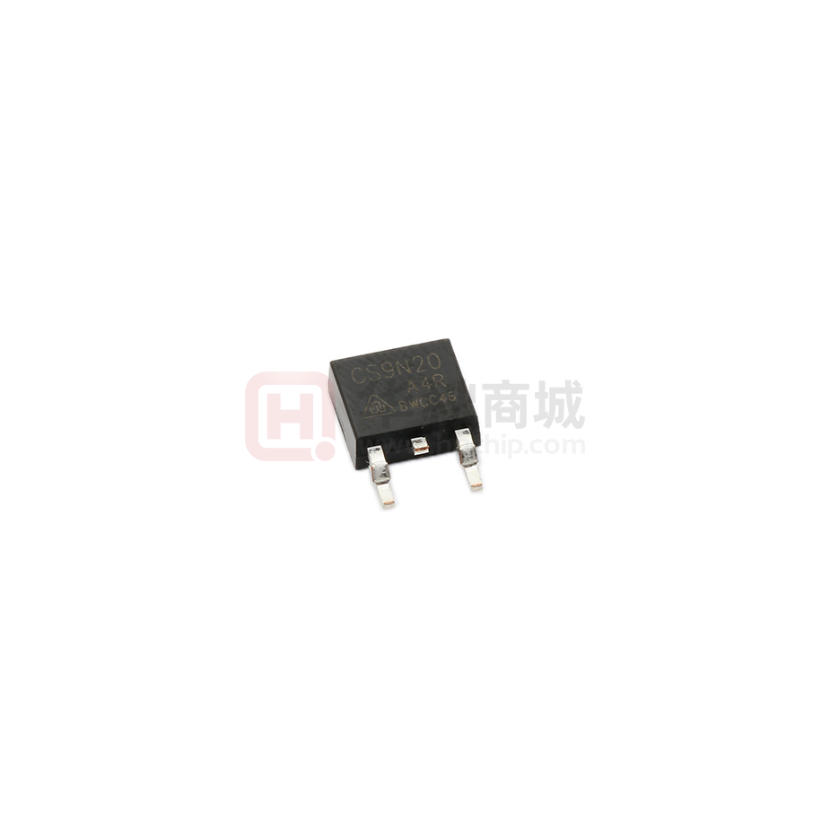
CS9N20 A4R
General Description :
200
V
ID
9
A
VDMOSFETs, is obtained by the self-aligned planar Technology
P D(TC=25℃)
75
W
which reduce the conduction loss, improve switching
RDS(ON)Typ
0.24
Ω
CS9N20 A4R, the silicon N-channel Enhanced
VDSS
performance and enhance the avalanche energy. The transistor
can be used in various power switching circuit for system
miniaturization and higher efficiency. The package form is TO-252,
which accords with the RoHS standard.
Features:
Fast Switching
Low ON Resistance(Rdson≤0.28Ω)
Low Gate Charge
(Typical Data: 12.6nC)
Low Reverse transfer capacitances(Typical: 8.8pF)
100% Single Pulse avalanche energy Test
Applications:
Power switch circuit of adaptor and charger.
Absolute(TJ= 25℃ unless otherwise specified):
Symbol
Parameter
VDSS
Drain-to-Source Voltage
ID
a1
IDM
VGS
EAS
a2
dv/dt
a3
PD
Rating
Units
200
V
Continuous Drain Current TC = 25 °C
9
A
Continuous Drain Current TC = 100 °C
5.4
A
Pulsed Drain Current TC = 25 °C
36
A
Gate-to-Source Voltage
±30
V
Single Pulse Avalanche Energy
200
mJ
Peak Diode Recovery dv/dt
5.0
V/ns
Power Dissipation TC = 25 °C
75
W
0.60
W/℃
150,–55 to 150
℃
300
℃
Derating Factor above 25°C
TJ,Tstg
Operating Junction and Storage Temperature Range
TL
Maximum Temperature for Soldering
W U X I C H I N A R E S O U R C E S H U A J I N G M I C R O E L E C T R O N I C S C O . , LT D .
P ag e 1 of 10
2 0 1 8 V0 1
�CS9N20 A4R
R
○
Electrical Characteristics(TJ= 25℃ unless otherwise specified):
OFF Characteristics
Symbol
Parameter
Test Conditions
VDSS
Drain to Source Breakdown Voltage
VGS=0V, ID=250µA
ΔBVDSS/ΔTJ
Bvdss Temperature Coefficient
ID=250uA,Reference25℃
IDSS
Drain to Source Leakage Current
VDS =200V, VGS= 0V,
TJ = 25℃
VDS =160V, VGS= 0V,
TJ = 125℃
IGSS(F)
Gate to Source Forward Leakage
IGSS(R)
Gate to Source Reverse Leakage
Rating
Unit
s
Min.
Typ.
Max.
200
--
--
--
0.25
--
V/℃
--
--
1
µA
--
--
100
µA
VGS =+30V
--
--
100
nA
VGS =-30V
--
--
-100
nA
V
ON Characteristics
Symbol
Parameter
Test Conditions
RDS(ON)
Drain-to-Source On-Resistance
VGS=10V,ID=4.5A
VGS(TH)
Gate Threshold Voltage
VDS = VGS, ID = 250µA
Rating
Units
Min.
Typ.
Max.
--
0.24
0.28
Ω
2.0
--
4.0
V
Pulse width tp≤300µs,δ≤2%
Dynamic Characteristics
Symbol
Parameter
Test Conditions
gfs
Forward Trans conductance
VDS=15V, ID =4.5A
Rg
Gate resistance
f = 1.0MHz
Ciss
Input Capacitance
Coss
Output Capacitance
Crss
Reverse Transfer Capacitance
VGS = 0V VDS = 25V
f = 1.0MHz
Rating
Min.
Typ.
Max.
--
5
--
Units
S
Ω
2.6
--
550
--
--
94
--
--
8.8
--
pF
Resistive Switching Characteristics
Symbol
Parameter
td(ON)
Turn-on Delay Time
tr
Rise Time
td(OFF)
Turn-Off Delay Time
tf
Fall Time
Qg
Total Gate Charge
Qgs
Gate to Source Charge
Qgd
Gate to Drain (“Miller”)Charge
Test Conditions
ID =9A VDD = 100V
R G =10Ω
ID =9A VDD =160V
VGS = 10V
W U X I C H I N A R E S O U R C E S H U A J I N G M I C R O E L E C T R O N I C S C O . , LT D .
Rating
Min.
Typ.
Max.
--
10.9
--
--
3.5
--
--
19.2
--
--
4.5
--
--
12.6
--
--
3.1
--
--
5.8
--
P ag e 2 of 10
Units
2 0 1 8 V0 1
ns
nC
�CS9N20 A4R
R
○
Source-Drain Diode Characteristics
Symbol
Parameter
IS
Continuous Source Current (Body Diode)
ISM
Maximum Pulsed Current (Body Diode)
VSD
Diode Forward Voltage
trr
Reverse Recovery Time
Test Conditions
Rating
Units
Min.
Typ.
Max.
--
--
9
A
--
--
36
A
--
--
1.5
V
--
112.7
--
ns
--
476
--
nC
--
8
--
A
TC = 25 °C
IS=9.0A,VGS=0V
IS=9.0A,Tj = 25℃
Qrr
Reverse Recovery Charge
IRRM
Reverse Recovery Current
dIF/dt=100A/us,
VGS=0V
Pulse width tp≤300µs,δ≤2%
Symbol
Parameter
Max.
Units
Rθ JC
Junction-to-Case
1.67
℃/W
Rθ JA
Junction-to-Ambient
100
℃/W
a1
:Repetitive rating; pulse width limited by maximum junction temperature
:L=10mH, I D=6.4A, Start TJ =25℃
a3
:ISD =9A,di/dt ≤100A/us,V DD≤BV DS, Start TJ=25℃
a2
W U X I C H I N A R E S O U R C E S H U A J I N G M I C R O E L E C T R O N I C S C O . , LT D .
P ag e 3 of 10
2 0 1 8 V0 1
�CS9N20 A4R
R
○
Characteristics Curve:
Figure 1 Maximum Forward Bias Safe Operating Area
Figure 3 Maximum Continuous Drain Current vs Case Temperature
Figure 2 Maximum Power dissipation vs Case Temperature
Figure 4 Typical Output Characteristics
Figure 5 Maximum Effective Thermal Impedance , Junction to Case
W U X I C H I N A R E S O U R C E S H U A J I N G M I C R O E L E C T R O N I C S C O . , LT D .
P ag e 4 of 10
2 0 1 8 V0 1
�CS9N20 A4R
Figure 6 Typical Transfer Characteristics
Figure 8 Typical Drain to Source ON Resistance
vs Drain Current
R
○
Figure 7 Typical Body Diode Transfer Characteristics
Figure 9 Typical Drian to Source on Resistance
vs Junction Temperature
W U X I C H I N A R E S O U R C E S H U A J I N G M I C R O E L E C T R O N I C S C O . , LT D .
P ag e 5 of 10
2 0 1 8 V0 1
�CS9N20 A4R
Figure 10 Typical Theshold Voltage vs Junction Temperature
Figure 12 Typical Capacitance vs Drain to Source Voltage
R
○
Figure 11 Typical Breakdown Voltage vs Junction Temperature
Figure 13 Typical Gate Charge vs Gate to Source Voltage
W U X I C H I N A R E S O U R C E S H U A J I N G M I C R O E L E C T R O N I C S C O . , LT D .
P ag e 6 of 10
2 0 1 8 V0 1
�CS9N20 A4R
R
○
Test Circuit and Waveform:
Figure 14. Gate Charge Test Circuit
Figure 16. Resistive Switching Test Circuit
Figure 15. Gate Charge Waveforms
Figure 17. Resistive Switching Waveforms
W U X I C H I N A R E S O U R C E S H U A J I N G M I C R O E L E C T R O N I C S C O . , LT D .
P ag e 7 of 10
2 0 1 8 V0 1
�CS9N20 A4R
Figure 18. Diode Reverse Recovery Test Circuit
Figure20.Unclamped Inductive Switching Test Circuit
R
○
Figure 19. Diode Reverse Recovery Waveform
Figure21.Unclamped Inductive Switching Waveform
W U X I C H I N A R E S O U R C E S H U A J I N G M I C R O E L E C T R O N I C S C O . , LT D .
P ag e 8 of 10
2 0 1 8 V0 1
�CS9N20 A4R
R
○
Package Information :
Items
Values(mm)
MIN
MAX
A
6.30
6.90
A1
0
0.13
B
5.70
6.30
C
2.10
2.50
D
0.30
0.60
E1
0.60
0.90
E2
0.70
1.00
F
0.30
0.60
G
0.70
1.20
L1
9.60
10.50
L2
2.70
3.10
H
0.60
1.00
M
5.10
5.50
N
2.09
2.49
R
0.3
T
1.40
1.60
Y
5.10
6.30
TO-252 Package
W U X I C H I N A R E S O U R C E S H U A J I N G M I C R O E L E C T R O N I C S C O . , LT D .
P ag e 9 of 10
2 0 1 8 V0 1
�CS9N20 A4R
R
○
The name and content of poisonous and harmful material in products
Hazardous Substance
Pb
Hg
Cr(VI)
PBB
PBDE
DIBP
DEHP
DBP
BBP
≤0.1%
≤0.1%
≤0.1%
≤0.1%
≤0.1%
≤0.1%
≤0.1%
≤0.1%
≤0.1%
Lead Frame
○
○
○
○
○
○
○
○
○
○
Molding
○
○
○
○
○
○
○
○
○
○
Compound
Chip
○
○
○
○
○
○
○
○
○
○
Wire Bonding
○
○
○
○
○
○
○
○
○
○
Solder
×
○
○
○
○
○
○
○
○
○
Limit
Cd
≤
0.01%
○:Means the hazardous material is under the criterion of 2011/65/EU.
Note
×:Means the hazardous material exceeds the criterion of 2011/65/EU.
The plumbum element of solder exist in products presently, but within the allowed range
of Eurogroup’s RoHS.
Warnings
1.
2.
3.
4.
Exceeding the maximum ratings of the device in performance may cause damage to the device,
even the permanent failure, which may affect the dependability of the machine. It is suggested
to be used under 80 percent of the maximum ratings of the device.
When installing the heat sink, please pay attention to the torsional moment and the smoothness
of the heat sink.
VDMOSFETs is the device which is sensitive to the static electricity, it is necessary to protect
the device from being damaged by the static electricity when using it.
This publication is made by Huajing Microelectronics and subject to regular change without
notice.
WUXI CHINA RESOURCES HUAJING MICROELECTRONICS CO., LTD.
Add: No.14 Liangxi RD. Wuxi, Jiangsu, China Mail:214061
http://www. crhj.com.cn
Tel: +86 0510-85807228 Fax: +86- 0510-85800864
HTU
Marketing Part:
Post:214061
UTH
Tel: +86 0510-81805277/81805336
Fax: +86 0510-85800360/85803016
Application and Service:Post:214061 Tel / Fax:+86- 0510-81805243/81805110
W U X I C H I N A R E S O U R C E S H U A J I N G M I C R O E L E C T R O N I C S C O . , LT D .
Page 10 of 10
2 0 1 8 V0 1
�
很抱歉,暂时无法提供与“CS9N20A4R”相匹配的价格&库存,您可以联系我们找货
免费人工找货