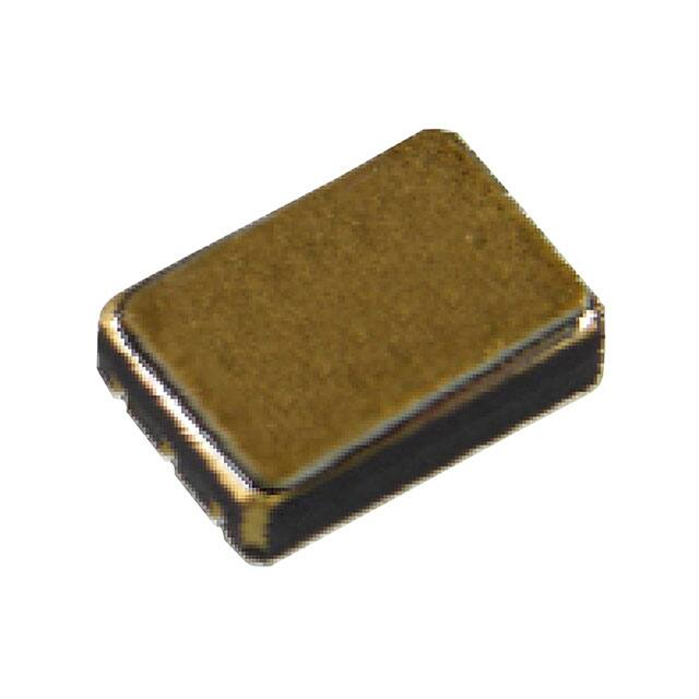
Dual Enhancement Mode
MOSFET
HCT802, HCT802TX, HCT802TXV
Features:
6 pad surface mount package
VDS = 90V
RDS(on) < 5Ω
ID(on) N-Channel = 1.5A | P-Channel = 1.1A
Two devices selected for VDS ID(on) and RDS(on) similarity
Full TX Processing Available
Gold plated contacts
Description:
HCT802 offers an N‐Channel and P‐Channel MOS transistor in a herme c ceramic surface mount package. The devices used
are similar to industry standards 2N6661 N‐Channel device and VP1008 P‐Channel device. These two enhancement mode
MOSFETS are par cularly well matched for VDS, IDS(on), RDS(on) and Gfs.
TX and TXV devices are processed to OPTEK’s military screening program pa erned a er MIL‐PRF‐19500.
TX products receive a VGS HTRB at 24 V for 48 hrs. at 150° C and a VDS HTRB at 48 V for 260 hrs.at 150° C.
Applications:
Drivers: Solid State
Relays, Lamps,
Solenoids, Displays,
Memories, etc.
Motor Control
Power Supply
Circuits
Part
Number
HCT801
HCT801TX
HCT801TXV
Sensor Type
VDSS
Min
ID(ON) (mA)
Min
N & P ‐Channel
Enhancement
MOSFET
90
1.5 & ‐1.1 170 & 200
General Note
TT Electronics reserves the right to make changes in product specification without
notice or liability. All information is subject to TT Electronics’ own data and is
considered accurate at time of going to print.
© TT electronics plc
Gfs (ms)
Min
t(ON) / t(OFF) (ns)
Max
Package
15/17 & 50/50
6‐pin Ceramic
OPTEK Technology, Inc.
1645 Wallace Drive, Carrollton, TX 75006|Ph: +1 972 323 2200
www.optekinc.com | www.ttelectronics.com
Issue A
11/2016 Page 1
�Dual Enhancement Mode
MOSFET
HCT802, HCT802TX, HCT802TXV
Absolute Maximum Ra ngs
Drain Source Voltage
90V
Gate‐Source Voltage
±20 V
Drain Current (Limited by Tj max) N‐Channel
P‐Channel
2A
1.1A
Opera ng and Storage Temperature
-55° C to +150° C
Power Dissipa on
TA = 25°C (Both devices equally driven)
0.5 W Total
TA = 25°C (Both devices equally driven)
1.5 W Total (1)
(TS = Substrate that the package is soldered to)
Electrical Characteris cs (TA = 25° C unless otherwise noted)
SYMBOL
PARAMETER
DEVICE
B=BOTH
MIN
MAX
UNITS
B
90(2)
V
ID = 10 µA(2), VGS = 0
N
0.75
2.5
V
VGS = VDS, ID = 1 mA
P
‐2.0
‐4.5
V
ID = ‐1 mA
B
±100
nA
VGS = ± 20 V, VDS = 0
B
10(2)
µA
VDS = 90 V(2), VGS = 0 V
B
500(2)
µA
Tj = 150° C
N
1.5
A
VDS = 25 V, VGS = 10 V
P
‐1.1
A
VDS = ‐15 V, VGS = ‐10 V
VGS = 10 V(2), ID = 1 A(2)
TEST CONDITIONS
BVDSS
Drain‐Source Breakdown
VTH
Gate Threshold Voltage
IGSS
Gate‐Body Leakage
IDSS
Zero Gate Voltage Drain Current
ID(on)
On‐State Drain Current
RDS(on)
Drain‐Source on Resistance
B
5
Ω
Gfs
Forward Transconductance
N
170
mmho
VDS = 25V, ID = 0.5 A
P
200
Mmho
VDS = ‐10 V, ID = ‐0.5 A
CISS
Input Capacitance
N
70
pf
VDS = 25 V, VGS = 0 V, f = 1 MHz
P
150
pf
VDS = ‐25 V, VGS = 0 V, f = 1 MHz
COSS
Common Source Output Capacitance
N
40
pf
VDS = 25 V, VGS = 0 V, f = 1 MHz
P
60
pf
VDS = ‐25 V, VGS = 0 V, f = 1 MHz
CRSS
Reverse Transfer Capacitance
N
10
pf
VDS = 25 V, VGS = 0 A, f = 1 MHz
P
25
pf
VDS = ‐25 V, VGS = 0 A, f = 1 MHz
Note:
1)
This ra ng is provided as an aid to designers. It is dependent upon moun ng material and methods and is not measurable as an outgoing test.
2)
Reverse polarity for P‐Channel device
General Note
TT Electronics reserves the right to make changes in product specification without
notice or liability. All information is subject to TT Electronics’ own data and is
considered accurate at time of going to print.
© TT electronics plc
OPTEK Technology, Inc.
1645 Wallace Drive, Carrollton, TX 75006|Ph: +1 972 323 2200
www.optekinc.com | www.ttelectronics.com
Issue A
11/2016
Page 2
�Dual Enhancement Mode
MOSFET
HCT802, HCT802TX, HCT802TXV
Electrical Characteris cs (TA = 25° C unless otherwise noted)
SYMBOL
PARAMETER
DEVICE
B=BOTH
MIN
MAX
UNITS
TEST CONDITIONS
t(on)
Turn‐on‐ me
N
15
ns
VDD = 25 v, ID = 1 A, RL = 50 Ω
P
50
ns
VDD = ‐25 v, ID = ‐0.5 A, RL = 50 Ω
t(off)
Turn‐off‐ me
N
17
ns
VDD = 25 v, ID = 1 A, RL = 50 Ω
P
50
ns
VDD = ‐25 v, ID = ‐0.5 A, RL = 50 Ω
General Note
TT Electronics reserves the right to make changes in product specification without
notice or liability. All information is subject to TT Electronics’ own data and is
considered accurate at time of going to print.
© TT electronics plc
OPTEK Technology, Inc.
1645 Wallace Drive, Carrollton, TX 75006|Ph: +1 972 323 2200
www.optekinc.com | www.ttelectronics.com
Issue A
11/2016
Page 3
�