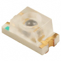
OP522

OP522

  • 厂商:

    IRCTT(TT电子)

  • 封装:

    1206

  • 描述:

    PHOTOTRANSISTOR NPN CLEAR 1206

  • 详情介绍
  • 数据手册
  • 价格&库存
OP522 数据手册
Silicon Phototransistor in Miniature SMT Package OP522 • • • High Photo Sensitivity Fast Response Time 1206 Package Size with Internal Lens The OP522 is an NPN silicon phototransistor mounted in a miniature SMT package. The device incorporates an integral molded lens which enables a narrow acceptance angle and higher collector currents than devices without lenses. This device is packaged in a 1206 size chip carrier that is compatible with most automated mounting equipment. The OP522 is mechanically and spectrally matched to the OP250 series infrared LEDs. Applications • • • • Non-Contact Position Sensing Datum detection Machine automation Optical encoders Relative Response vs. Wavelength 100% OP522 Relative Response 80% 60% 40% 20% 0% 400 500 600 700 800 900 1000 1100 Wavelength (nm) RoHS OPTEK reserves the right to make changes at any time in order to improve design and to supply the best product possible. OPTEK Technology Inc.— 1645 Wallace Drive, Carrollton, Texas 75006 Phone: (800) 341-4747 FAX: (972) 323– 2396 sensors@optekinc.com www.optekinc.com Issue A 12/2010 Page 1 of 4 SMT Silicon Phototransistor OP522 Absolute Maximum Ratings TA = 25o C unless otherwise noted Storage Temperature Range -40° C to +85° C Operating Temperature Range -25° C to +85° C 260° C(1) Lead Soldering Temperature Collector-Emitter Voltage 30 V Emitter-Collector Voltage 5V Collector Current 20 mA 75 mW(2) Power Dissipation Notes: 1. Solder time less than 5 seconds at temperature extreme. 2. De-rate linearly at 2.17 mW/° C above 25° C. Electrical Characteristics (TA = 25°C unless otherwise noted) SYMBOL PARAMETER IC(ON) On-State Collector Current VCE(SAT) ICEO TYP MAX UNITS 0.5 CONDITIONS mA VCE = 5.0V, Ee = 5.0mW/cm2 (3) Collector-Emitter Saturation Voltage 0.4 V IC = 100µA, Ee = 2.0mW/cm2 (3) Collector-Emitter Dark Current 100 nA VCE = 5.0V, Ee = 0 (4) V(BR)CEO Collector-Emitter Breakdown Voltage 30 V IC = 100µA V(BR)ECO Emitter-Collector Breakdown Voltage 5 V IE = 100µA µs IC = 1mA, RL = 1KΩ tr, tf Rise and Fall Times 15 Light source is an unfiltered GaAs LED with a peak emission wavelength of 935nm and a radiometric intensity level which varies less than 10% over the entire lens surface of the phototransistor being tested. (0.04 T -3/4) where TA is the ambient temperature in ° C. To Calculate typical collector dark current in µA, use the formula ICEO = 10 A 4. 160% Relative Collector Current 140% Relative On-State Collector Current vs. Irradiance Relative On-State Collector Current vs. Temperature 140% Normalized at Ee = 5mW/cm2 Conditions: VCE = 5V, λ = 935nm, TA = 25 °C 130% Relative Collector Current 3. MIN 120% 100% 80% 60% 40% 20% 0 Normalized at TA = 25°C . Conditions: VCE = 5V, λ = 935nm, TA = 25 °C 120% 110% 100% 90% 80% 70% 1.0 2.0 3.0 4.0 5.0 6.0 2 Ee—Irradiance (mW/cm ) 7.0 8.0 -25 0 25 50 75 100 Temperature—(°C) OPTEK reserves the right to make changes at any time in order to improve design and to supply the best product possible. Issue A 12/2010 Page 2 of 4 OPTEK Technology Inc.— 1645 Wallace Drive, Carrollton, Texas 75006 Phone: (800) 341-4747 FAX: (972) 323– 2396 sensors@optekinc.com www.optekinc.com SMT Silicon Phototransistor OP522 Relative Response vs. Angular Position Relative On-State Collector Current vs. Collector-Emitter Voltage 100% IC(ON) - On-State Collector Current (mA) 2.00 Relative Response 80% 60% 40% 20% 1.80 6 mW/cm2 1.60 5 mW/cm2 1.40 4 mW/cm2 1.20 1.00 3 mW/cm2 0.80 2 mW/cm2 0.60 0.40 1 mW/cm2 0.20 0% -90 -60 -30 0 30 60 90 0 Angular Position (Degrees) 0.1 0.2 0.3 0.4 0.5 Collector-Emitter Voltage (V) Collector-Emitter Dark Current vs. Temperature Collector-Emitter Dark Current (nA) 1000 Conditions: Ee = 0 mW/cm2 VCE = 10V 100 10 1 0 -25 0 25 50 75 100 Temperature—(°C) OPTEK reserves the right to make changes at any time in order to improve design and to supply the best product possible. OPTEK Technology Inc.— 1645 Wallace Drive, Carrollton, Texas 75006 Phone: (800) 341-4747 FAX: (972) 323– 2396 sensors@optekinc.com www.optekinc.com Issue A 12/2010 Page 3 of 4 SMT Silicon Phototransistor OP522 2 1 RECOMMENDED SOLDER PADS [4.60±0.10] .181±.0039 [1.50±0.10] .059±.0039 [1.60±0.10] .063±.0039 PIN [1.60±0.10] .063±.0039 FUNCTION 1 Collector 2 Emitter OPTEK reserves the right to make changes at any time in order to improve design and to supply the best product possible. Issue A 12/2010 Page 4 of 4 OPTEK Technology Inc.— 1645 Wallace Drive, Carrollton, Texas 75006 Phone: (800) 341-4747 FAX: (972) 323– 2396 sensors@optekinc.com www.optekinc.com
OP522
物料型号:OP522

器件简介: - OP522是一款NPN硅光晶体管,采用微型SMT封装。 - 该器件内置了一个整体成型的透镜,能够实现狭窄的接收角度和比无透镜设备更高的集电极电流。 - 与OP250系列红外LED在机械和光谱上匹配。

引脚分配: - 引脚1:集电极(Collector) - 引脚2:发射极(Emitter)

参数特性: - 存储温度范围:-40°C至+85°C - 工作温度范围:-25°C至+85°C - 焊接温度:260°C - 集电极-发射极电压:30V - 发射极-集电极电压:5V - 集电极电流:20mA - 功率耗散:75mW(在25°C时)

功能详解: - 该光晶体管适用于非接触式位置传感、基准检测、机器自动化和光学编码器等应用。 - 相对响应与波长的关系图显示了在不同波长下的相对响应。 - 相对开启状态下的集电极电流与辐照度的关系图显示了在不同辐照度下的集电极电流变化。 - 相对开启状态下的集电极电流与温度的关系图显示了在不同温度下的集电极电流变化。 - 相对开启状态下的集电极电流与集电极-发射极电压的关系图显示了在不同电压下的集电极电流变化。 - 相对响应与角度位置的关系图显示了在不同角度位置下的相对响应。

应用信息: - 非接触式位置传感 - 基准检测 - 机器自动化 - 光学编码器

封装信息: - 封装尺寸为1206,与大多数自动化安装设备兼容。

注意事项: - OPTEK Technology保留随时更改设计的权利,以提供最佳产品。

联系信息: - OPTEK Technology Inc., 1645 Wallace Drive, Carrollton, Texas 75006 - 电话:(800) 341-4747 - 传真:(972) 323– 2396 - 邮箱:sensors@optekinc.com - 网站:www.optekinc.com
OP522 价格&库存

很抱歉,暂时无法提供与“OP522”相匹配的价格&库存,您可以联系我们找货

免费人工找货