Bulletin I25201 rev. B 03/03
80RIA SERIES
PHASE CONTROL THYRISTORS Stud Version
Features
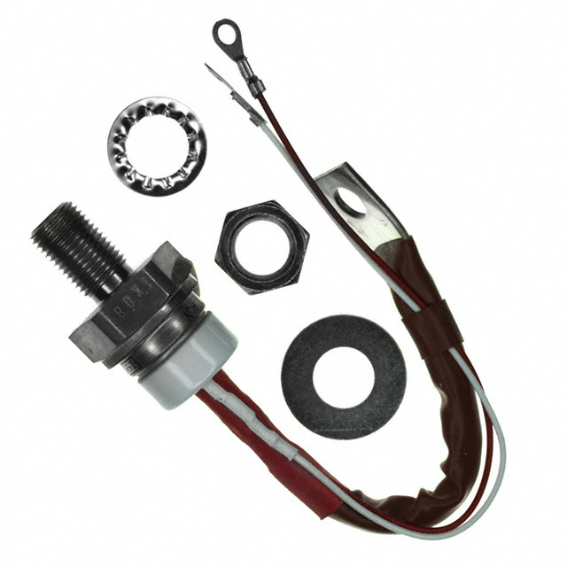
Hermetic glass-metal seal International standard case TO-209AC (TO-94)
80A
Typical Applications
DC motor controls Controlled DC power supplies AC controllers
Major Ratings and Characteristics
Parameters
IT(AV) @ TC IT(RMS) ITSM @ 50Hz @ 60Hz I 2t @ 50Hz @ 60Hz V DRM /V RRM tq TJ typical
80RIA
80 85 125 1900 1990 18 16 400 to 1200 110 - 40 to 125
Unit
A °C A A A KA2s KA2s V µs °C
case style TO-209AC (TO-94)
www.irf.com
1
�8 0RIA Series
Bulletin I25201 rev. B 03/03
ELECTRICAL SPECIFICATIONS Voltage Ratings
Voltage Type number Code
40 80RIA 80 120
V DRM/V RRM, max. repetitive peak and off-state voltage V
400 800 1200
VRSM , maximum nonrepetitive peak voltage V
500 900 1300
I DRM/I RRM m ax.
@ TJ = 125°C
mA
15
On-state Conduction
Parameter
I T(AV) Max. average on-state current @ Case temperature I T(RMS) Max. RMS on-state current I TSM Max. peak, one-cycle non-repetitive surge current
80RIA
80 85 125 1900 1990 1600 1675
Units
A °C A
Conditions
180° conduction, half sine wave
DC @ 75°C case temperature t = 10ms No voltage reapplied 100% VRRM reapplied No voltage reapplied 100% VRRM reapplied Sinusoidal half wave, Initial TJ = TJ max.
A
t = 8.3ms t = 10ms t = 8.3ms t = 10ms
I2t
Maximum I2t for fusing
18 16 12.7 11.7 KA2 s
t = 8.3ms t = 10ms t = 8.3ms
I 2√ t
Maximum I2√t for fusing
180.5 0.99
KA2√s
t = 0.1 to 10ms, no voltage reapplied (16.7% x π x IT(AV) < I < π x IT(AV)), TJ = TJ max.
V T(TO)1 Low level value of threshold voltage V T(TO) 2 High level value of threshold voltage r t1 r t2 V TM IH IL Low level value of on-state slope resistance High level value of on-state slope resistance Max. on-state voltage Maximum holding current Typical latching current
V 1.13 (I > π x IT(AV)),TJ = TJ max. (16.7% x π x IT(AV) < I < π x IT(AV)), TJ = TJ max. mΩ 1.84 1.60 200 400 mA T J = 2 5°C, anode supply 12V resistive load V (I > π x IT(AV)),TJ = TJ max. Ipk= 250A, TJ = 25°C tp = 10ms sine pulse
2.29
2
www.irf.com
�8 0RIA Series
Bulletin I25201 rev. B 03/03
Switching
Parameter
di/dt Max. non-repetitive rate of rise of turned-on current 300 A/µs
80RIA
Units
Conditions
TJ = 125°C, Vd = rated VDRM, ITM = 2xdi/dt snubber Per JEDEC Standard RS-397, 5.2.2.6. 0.2µF, 15Ω, Gate pulse: 20V, 65Ω, tp = 6µs, tr= 0.5µs
td tq
Typical delay time
1 µs
Gate pulse: 10V, 15Ω source, tp = 6µs, tr = 0.1µs, Vd = rated VDRM, ITM = 50Adc, TJ = 25°C. dv/dt = 20V/µs, Gate bias: 0V 25Ω, tp = 500µs ITM = 50A, TJ = TJ max, di/dt = -5A/µs min., VR = 50V,
Typical turn-off time
110
Blocking
Parameter
dv/dt IRRM IDRM Maximum critical rate of rise of off-state voltage Max. peak reverse and off-state leakage current
80RIA
500 15
Units
V/µs mA
Conditions
TJ = 125°C exponential to 67% rated VDRM TJ = 125°C rated V DRM /V RRM applied
Triggering
Parameter
PGM Maximum peak gate power
80RIA
12 3 3 20
Units
W A
Conditions
TJ = TJ max, t p ≤ 5 ms TJ = TJ max, f = 50Hz, d% = 50 TJ = TJ max, t p ≤ 5 ms
PG(AV) Maximum average gate power IGM +VGM -VGM Max. peak positive gate current Maximum peak positive gate voltage Maximum peak negative gate voltage IGT Max. DC gate current required to trigger
V 10 270 120 60 mA
TJ = TJ max, tp ≤ 5ms
TJ = - 40°C TJ = 25°C TJ = 125°C TJ = - 40°C V TJ = 25°C TJ = 125°C mA TJ = TJ max Max. gate current/ voltage not to trigger is the max. value which will not trigger any unit with rated VDRM anode-to-cathode applied Max. required gate trigger/ current/ voltage are the lowest value which will trigger all units 6V anode-to-cathode applied
VGT
Max. DC gate voltage required to trigger
3.5 2.5 1.5
IGD VGD
DC gate current not to trigger
6
DC gate voltage not to trigger
0.25
V
www.irf.com
3
�8 0RIA Series
Bulletin I25201 rev. B 03/03
Thermal and Mechanical Specification
Parameter
TJ Tstg Max. operating temperature range Max. storage temperature range
80RIA
-40 to 125 -40 to 150 0.30
Units
°C
Conditions
RthJC Max. thermal resistance, junction to case RthCS Max. thermal resistance, case to heatsink T Mounting torque, ± 10%
DC operation K/W
0.1 15.5 (137) 14 (120) Nm (lbf-in) g
Mounting surface, smooth, flat and greased Non lubricated threads Lubricated threads
wt
Approximate weight Case style
130
TO-209AC(TO-94)
See Outline Table
∆RthJ-C Conduction
(The following table shows the increment of thermal resistence RthJ-C when devices operate at different conduction angles than DC)
Conduction angle
180° 120° 90° 60° 30°
Sinusoidal conduction Rectangular conduction Units
0.042 0.050 0.064 0.095 0.164 0.030 0.052 0.070 0.100 0.165 K/W
Conditions
T J = T J m ax.
Ordering Information Table
Device Code
8
1
0
2
RIA 120
3 4
1 2
-
ITAV x 10A 0 = Eyelet terminals (Gate and Auxiliary Cathode Leads) 1 = Fast - on terminals (Gate and Auxiliary Cathode Leads)
3 4 5
-
RIA = Essential part number Voltage code: Code x 10 = VRRM (See Voltage Rating Table) None = Stud base 1/2"-20UNF- 2A threads NOTE: For Metric Device M12 x 1.75 E6 Contact factory
4
www.irf.com
�8 0RIA Series
Bulletin I25201 rev. B 03/03
Outline Table
GLASS METAL SEAL
16.5 (0.65) MAX. 8.5 (0.3) DIA. 4.3 (0.17) DIA.
37 )M IN. ( 0. 9 .5
2.5 (0.10) MAX.
C.S. 16mm 2 (.025 s.i.) RED SILICON RUBBER 157 (6.18) 170 (6.69) RED CATHODE WHITE GATE C.S. 0.4 mm (.0006 s.i.) 2
20
(0 .
FLEXIBLE LEAD
79
)M
IN.
Fast-on Terminals
AMP. 280000-1 REF-250
55 (2.17) MIN.
215 (8.46) RED SHRINK WHITE SHRINK 24 (0.94) MAX.
10 (0.39)
10 (0.39) MAX.
23.5 (0.92) MAX. DIA.
21 (0.83)
MAX.
SW 27 1/2"-20UNF-2A * 29.5 (1.16) MAX.
Case Style TO-209AC (TO-94)
All dimensions in millimeters (inches)
* FOR METRIC DEVICE: M12 X 1.75 E6 CONTACT FACTORY
Maximum Allowable Case T emperature (°C)
130 80RIA S eries RthJC (DC) = 0.30 K/ W 120
Maximum Allowable Case T emperature (°C)
130 120 110
80RIA S eries RthJC (DC) = 0.30 K/ W
110
Conduc tion Angle
Conduction Period
100 90 30° 80 70 0 20 40 60 80 100 120 140 Average On-state Current (A)
Fig. 2 - Current Ratings Characteristics
100
30°
60° 90° 120° 180°
90
60° 90° 120° 180° DC
80 0 10 20 30 40 50 60 70 80 90 Average On-s tate Current (A)
Fig. 1 - Current Ratings Characteristics
www.irf.com
5
�8 0RIA Series
Bulletin I25201 rev. B 03/03
Maximum Average On-s tate Power Loss (W) 120
hS Rt
110 100
90
80 70
60 50
180° 120° 90° 60° 30° RMSLimit
6 0. W K/
A
= W K/ 0.4
1
K/ W
-D elt a
1.4 K/ W
2K /W
R
40 30
20
Conduction Angle
3 K/
W
10 0
0 10 20 30 40
80RIA S eries T = 125°C J
50 60 70 80 0
5 K/ W
25
50
75
100
125
Average On-state Current (A)
Maximum Allowable Ambient T emperature (°C)
Fig. 3 - On-state Power Loss Characteristics
Maximum Average On-state Power Los (W) s
180 160 140
120 100 80 60
40 20 0
DC 180° 120° 90° 60° 30°
R
th S A
=
0. 6
0. 4
K/ W
K/ W
-D el ta
1K /W
R
RMSLimit
Conduc tion Period
1.4 K/ W
2 K/ W
3 K/ W
80RIA S eries T = 125°C J 0 20 40 60 80 100 120
5 K/ W
140 0
25
50
75
100
125
Average On-state Current (A)
Maximum Allowable Ambient T emperature (°C)
Fig. 4 - On-state Power Loss Characteristics
Peak Half S Wave On-s ine tate Current (A)
1600
At Any R ated Load Condition And With R ated VRRM Applied Following S urge. Initial T = 125°C J @60 Hz 0.0083 s @50 Hz 0.0100 s
1400
Peak Half S Wave On-state Current (A) ine
1800
2000 Maximum Non Repetitive S urge Current 1900 Versus Pulse T rain Duration. Control 1800 Of Conduction May Not Be Maintained. Initial T = 125°C 1700 J No Voltage Reapplied 1600 Rated VRRM Reapplied 1500 1400 1300 1200 1100 1000 900 80RIA S eries 800 700 0.01
1200
1000 80R S IA eries 800 1 10 100
Number Of Equa l Amplitude Half Cycle Current Pulses (N)
0.1
1
Puls T e rain Duration (s)
Fig. 6 - Maximum Non-Repetitive Surge Current
Fig. 5 - Maximum Non-Repetitive Surge Current
6
www.irf.com
�8 0RIA Series
Bulletin I25201 rev. B 03/03
10000 Instantaneous On-state Current (A)
1000
100 T = 25°C J T = 125°C J 10 80R S IA eries 1 0.5 1 1.5 2 2.5 3 3.5 4 4.5 5
Instantaneous On-state Voltage (V)
Fig. 7 - On-state Voltage Drop Characteristics
1 S teady S tate Value R thJC = 0.30 K/ W (DC Operation) 0.1
T ransient T hermal Impedance Z
thJC
(K/ W)
0.01
80RIA S eries 0.001 0.0001
0.001
0.01
0.1
1
10
S uare Wave Pulse Duration (s) q
Fig. 8 - Thermal Impedance ZthJC Characteristics
100 Instantaneous Gate Voltage (V)
Rectangular gate pulse a) R ecommended load line for rated di/ dt : 20V, 30ohms; tr
很抱歉,暂时无法提供与“80RIA80”相匹配的价格&库存,您可以联系我们找货
免费人工找货