PD -2.339
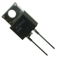
HFA25TB60
HEXFRED
Features
TM
Ultrafast, Soft Recovery Diode
VR = 600V VF (typ.)* = 1.3V IF(AV) = 25A Qrr (typ.)= 112nC IRRM = 10A trr(typ.) = 23ns di(rec)M/dt (typ.) = 250A/µs
Benefits
Ultrafast Recovery Ultrasoft Recovery Very Low IRRM Very Low Qrr Guaranteed Avalanche Specified at Operating Conditions
Reduced RFI and EMI Reduced Power Loss in Diode and Switching Transistor Higher Frequency Operation Reduced Snubbing Reduced Parts Count
Description
International Rectifier's HFA25TB60 is a state of the art ultra fast recovery diode. Employing the latest in epitaxial construction and advanced processing techniques it features a superb combination of characteristics which result in performance which is unsurpassed by any rectifier previously available. With basic ratings of 600 volts and 25 amps continuous current, the HFA25TB60 is especially well suited for use as the companion diode for IGBTs and MOSFETs. In addition to ultra fast recovery time, the HEXFRED product line features extremely low values of peak recovery current (IRRM) and does not exhibit any tendency to "snap-off" during the tb p ortion of recovery. The HEXFRED features combine to offer designers a rectifier with lower noise and significantly lower switching losses in both the diode and the switching transistor. These HEXFRED advantages can help to significantly reduce snubbing, component count and heatsink sizes. The HEXFRED HFA25TB60 is ideally suited for applications in power supplies and power conversion systems (such as inverters), motor drives, and many other similar applications where high speed, high efficiency is needed.
TO-220AC
Absolute Maximum Ratings
Parameter
VR IF @ T C = 25°C IF @ T C = 100°C IFSM IFRM IAR PD @ TC = 25°C PD @ TC = 100°C TJ TSTG Cathode-to-Anode Voltage Continuous Forward Current Continuous Forward Current Single Pulse Forward Current Maximum Repetitive Forward Current Maximum Repetitive Avalanche Current Maximum Power Dissipation Maximum Power Dissipation Operating Junction and Storage Temperature Range
Max.
600 25 225 100 2.0 125 50 -55 to +150
Units
V
A
W C
* 125°C
4/2/97
�HFA25TB60
Electrical Characteristics @ TJ = 25°C (unless otherwise specified)
Parameter
VBR VFM I RM CT LS Cathode Anode Breakdown Voltage Max Forward Voltage Max Reverse Leakage Current Junction Capacitance Series Inductance
Min. Typ. Max. Units
600 1.3 1.7 1.5 2.0 1.3 1.7 1.5 20 600 2000 55 100 8.0 V V µA pF nH
Test Conditions
IR = 100µA IF = 25A See Fig. 1 IF = 50A IF = 25A, T J = 125°C See Fig. 2 VR = VR Rated TJ = 125°C, VR = 0.8 x VR R atedD Rated See Fig. 3 VR = 200V Measured lead to lead 5mm from package body
Dynamic Recovery Characteristics @ TJ = 25°C (unless otherwise specified)
Parameter
trr trr1 trr2 IRRM1 IRRM2 Qrr1 Qrr2 di(rec)M/dt1 di(rec)M/dt2 Reverse Recovery Time See Fig. 5, 6 & 16 Peak Recovery Current See Fig. 7& 8 Reverse Recovery Charge See Fig. 9 & 10 Peak Rate of Fall of Recovery Current During tb See Fig. 11 & 12
Min. Typ. Max. Units
23 50 75 ns 105 160 4.5 10 A 8.0 15 112 375 nC 420 1200 250 A/µs 160
Test Conditions
IF = 1.0A, dif /dt = 200A/µs, VR = 30V TJ = 25°C TJ = 125°C I F = 25A TJ = 25°C TJ = 125°C V R = 200V TJ = 25°C TJ = 125°C dif/dt = 200A/µs TJ = 25°C TJ = 125°C
Thermal - Mechanical Characteristics
Parameter
Tlead Rθ JC RθJA RθCS Wt Lead Temperature Thermal Resistance, Junction to Case Thermal Resistance, Junction to Ambient Thermal Resistance, Case to Heat Sink Weight Mounting Torque
Min.
6.0 5.0
Typ.
0.5 2.0 0.07
Max.
300 1.0 80 12 10
Units
°C K/W g (oz) Kg-cm lbfin
L=100µH, duty cycle limited by max TJ 0.063 in. from Case (1.6mm) for 10 sec Typical Socket Mount Mounting Surface, Flat, Smooth and Greased
�HFA25TB60
100
10000
Reverse Current - IR (µA)
T = 150°C J
1000 100 10 1 0.1 0.01 0 100 200 300 400 500
TJ= 125°C
Instantaneous Forward Current - I F (A)
TJ = 150°C T = 125°C
J J
TJ = 25°C
A 600
T = 25°C
10
Reverse Voltage - V R (V)
Fig. 2 - Typical Reverse Current vs. Reverse Voltage
1000
A
Junction Capacitance -CT (pF)
T = 25°C J
100
1 0.6
A 1.0 1.4 1.8 2.2 2.6
Forward Voltage Drop - V FM (V)
Fig. 1 - Maximum Forward Voltage Drop vs. Instantaneous Forward Current
10 1 10 100
A 1000
Reverse Voltage - VR (V)
Fig. 3 - Typical Junction Capacitance vs. Reverse Voltage
10
Thermal Response (Z thJC)
1 D = 0.50 0.20 0.1 0.10 0.05 0.02 0.01 SINGLE PULSE (THERMAL RESPONSE) PDM t1 t2 Notes: 1. Duty factor D = t1 / t 2 2. Peak T J = P DM x Z thJC + TC 0.001 0.01 0.1 1
0.01 0.00001
0.0001
t1, Rectangular Pulse Duration (sec)
Fig. 4 - Maximum Thermal Impedance Zthjc Characteristics
�HFA25TB60
140 VR = 200V TJ = 125°C TJ = 25°C 120
25 30 VR = 200V TJ = 125°C TJ = 25°C
100
20
I F = 50A I F = 25A I F = 10A
trr- (nC)
80
I F = 50A I F = 25A I F = 10A
Irr- ( A)
A
15
60
10
40
5
20 100
di f /dt - (A/µs)
1000
0 100
A
di f /dt - (A/µs)
1000
Fig. 5 - Typical Reverse Recovery vs. dif/dt
1400 VR = 200V TJ = 125 °C TJ = 25°C
Fig. 6 - Typical Recovery Current vs. dif/dt
10000 VR = 200V TJ = 125°C TJ = 25°C
1200
1000
I F = 50A I F = 25A IF = 10A
800
di (rec) M/dt- (A /µs)
Qrr- (nC)
1000
I F = 50A I F = 25A I F = 10A
600
400
200
A 0 100
di f /dt - (A/µs)
1000
100 100
A
di f /dt - (A/µs)
1000
Fig. 7 - Typical Stored Charge vs. di f/dt
Fig. 8 - Typical di(rec)M/dt vs. dif/dt
�HFA25TB60
3
IF
t rr ta tb
4
REVERSE RECOVERY CIRCUIT
VR = 200V
0 Q rr I RRM
2
0.5 I RRM di(rec)M/dt
5
0.01 Ω L = 70µH D.U.T. D IRFP250 S
1
0.75 I RRM di f /dt
4. Qrr - Area under curve defined by trr and I RRM t rr X IRRM Qrr = 2
dif/dt ADJUST G
1. dif/dt - Rate of change of current through zero crossing 2. IRRM - Peak reverse recovery current
3. trr - Reverse recovery time measured 5. di(rec)M/dt - Peak rate of change of from zero crossing point of negative current during tb portion of trr going IF to point where a line passing through 0.75 IRRM and 0.50 I RRM extrapolated to zero current
Fig. 9 - Reverse Recovery Parameter Test Circuit
Fig. 10 - Reverse Recovery Waveform and Definitions
L = 100µH HIGH-SPEED SWITCH Rg = 25 ohm CURRENT MONITOR FREE-WHEEL DIODE + Vd = 50V
I L(PK)
DUT
DECAY TIME V (AVAL) V R(RATED)
Fig. 11 - Avalanche Test Circuit and Waveforms
�HFA25TB60
Conforms to JEDEC Outline TO-220AC Dimensions in millimeters and inches
WORLD HEADQUARTERS: 233 Kansas St., El Segundo, California 90245, Tel: (310) 322 3331 EUROPEAN HEADQUARTERS: Hurst Green, Oxted, Surrey RH8 9BB, UK Tel: ++ 44 1883 732020 IR CANADA: 7321 Victoria Park Ave., Suite 201, Markham, Ontario L3R 2Z8, Tel: (905) 475 1897 IR GERMANY: Saalburgstrasse 157, 61350 Bad Homburg Tel: ++ 49 6172 96590 IR ITALY: Via Liguria 49, 10071 Borgaro, Torino Tel: ++ 39 11 451 0111 IR FAR EAST: K&H Bldg., 2F, 30-4 Nishi-Ikebukuro 3-Chome, Toshima-Ku, Tokyo Japan 171 Tel: 81 3 3983 0086 IR SOUTHEAST ASIA: 315 Outram Road, #10-02 Tan Boon Liat Building, Singapore 0316 Tel: 65 221 8371 http://www.irf.com/ Data and specifications subject to change without notice. 4/97
�
很抱歉,暂时无法提供与“HFA25TB60”相匹配的价格&库存,您可以联系我们找货
免费人工找货