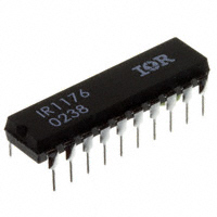
IR1176

IR1176

  • 厂商:

    IRF

  • 封装:

  • 描述:

    IR1176 - SYNCHRONOUS RECTIFIER DRIVER - International Rectifier

  • 详情介绍
  • 数据手册
  • 价格&库存
IR1176 数据手册
Preliminary Data Sheet PD60185-C IR1176 SYNCHRONOUS RECTIFIER DRIVER Features • Provides constant and proper gate drive to power Product Summary Vdd IO+/- (peak) Fmax Max lead time 5Vdc 4A/4A 2MHz 500nsec • • • • • • MOSFETs regardless of transformer output Minimizes loss due to power MOSFET body drain diode conduction Stand alone operation - no ties to primary side Schmitt trigger input with double pulse suppression allows operation in noisy environments High peak current drive capability - 4A High speed operation - 2MHz Adaptable to multiple topologies Description The IR1176 is a high speed CMOS controller designed to drive N-channel power MOSFETs used as synchronous rectifiers in high current, high frequency forward converters with output voltages equal or below 5VDC. Schmitt trigger inputs with double pulse suppression allow the controller to operate in noisy environments. The circuit does not require any ties to the primary side and derives its operating power directly from the secondary. The circuit functions by anticipating transformer output transitions, then turns the power MOSFETs on or off before the transitions of the transformer to minimize body drain diode conduction and reduce associated losses. Turn on/off lead time can be adjusted to accommodate a variety of power MOSFET sizes and circuit conditions. The IR1176 also provides gate drive overlap/dead-time control via external components to further minimize diode conduction by nulling effects of secondary loop and device package inductance. Packages IR1176S 20 Lead Surface Mount (SSOP-20) IR1176SS 20 Lead SOIC (MS-013AC) IR1176 20 Lead PDIP (MS-001AD) IR1176 Absolute Maximum Ratings Absolute maximum ratings indicate sustained limits beyond which damage to the device may occur. Symbol Vdd Iin PD Definition Supply voltage Input clamp current Power dissipation (SSOP-20) (SOIC) (PDIP) Min. — — — — — — — — — — — — -55 — Max. 7 +/- 10 400 — — 28.5 20 28.1 90.5 45 62.4 150 150 300 Units VDC mA DC mW — — RthJC Thermal resistance (SSOP-20) junction-to-case (SOIC) junction-to-case (PDIP) junction-to-case °C/W RthJA Thermal resistance (SSOP-20) junction-to-ambient (SOIC) junction-to-ambient (PDIP) junction-to-ambient TJ TS TL Junction temperature Storage temperature Lead temperature (soldering, 10 seconds) °C Recommended Operating Conditions Symbol Vdd TA Freq Rbias UV Xin Cd1/Cd2 Definition Supply voltage operating range Ambient temperature Operating frequency Required bias resistor (+/- 1%) Voltage at UVSET pin Maximum voltage at X1 and X2 inputs Capacitance at pins DTIN1 and DTIN2 Min. — -40 250 — 1.75 — — Typ. 5 — — 34.0 — — — Max. — 85 500 — 2.25 5.6 100 Units VDC °C KHz KΩ VDC VDC pF 2 www.irf.com IR1176 Dynamic Electrical Characteristics Vdd=5V, TA = 2 5 o C, Rbias = 34.0K unless otherwise specified. Symbol Vdd Iqdd Freq UVSET+ UVSETVxth+ VxthTadv Td Isink (peak) Isource (peak) VOH VOL tio Definition Supply voltage operating range Vdd quiescent current (x1 = x2 = 0V or 5V, Iout = 0) Operating frequency UVSET positive going threshold UVSET negative going threshold X1/X2 Input positive going threshold X1/X2 Input negative going threshold Externally adjustable lead time (advance) Externally adjustable dead-time for Q1 and Q2 Q1,Q2 output sink current (Vdd=5.0V, pulsed, 10 usec) Q1,Q2 output source current (Vdd=5.0V, pulsed, 10 usec) Q1, Q2 High level voltage (Iout = 20mA) Q1, Q2 Low level voltage (Iout = 20mA) Input to output delay (PLL bypassed, cross coupled mode) Min. 4.0 — 100 1.10 0.8 — — — 20 — Typ. — 4 — — — 1.4 1.0 — — 4 Max. 5.25 5 2000 1.4 1.1 — — 500 — — Units VDC A KHz V V VDC VDC nsec nsec — 4 — A — — — Vdd- 0.20 0.10 20 — — — V nsec tr tf Vtr Gate turn-on rise time (C1=1000pf, Vdd=5V) Gate turn-off fall time (C1=1000pf, Vdd=5V) Cross-over voltage (Vdd=5Vdc, DTIN shorted to DTOUT, C1=1000pf) Fig. 3 — — — 20 20 2.5 — — — nsec nsec VDC KΩ VDC nsec µA DC VDC KHz/ Volt Rbias Vbias Tjitter Ichgpump Vchgpump Kvco_dc Required bias resistor (1%) Voltage at Rbias pin Phase-lock loop output jitter Charge pump output current (at VFLTR pin) Charge pump output voltage (at VFLTR pin) PLL Vco DC gain (per design) — — -20 — 1.3 — 34.0 1.25 — 50 1.5 62 — — 20 — 1.7 — www.irf.com 3 IR1176 Lead Definitions and Assignments Symbol Description AVDD Q1 DTIN1 RADV1 VFLTR1 RVCO1 X1 VDD UVSET RBIAS AVSS X2 RVCO2 VFLTR2 RADV2 DTIN2 VSS Q2 Power - + 5 VDC to MOSFET drivers Output - gate drive for Q1 power MOSFET Input - sets dead time for Q1 - used with DTOUT1 Output - sets lead time (advance) for Q1 Output - PLL loop filter for Q1 output Output - sets PLL center frequency for Q1 output Input - transformer input for Q1 Power - +5 Vdc for internal logic Input - sets UVLO+ If this pin is pulled below 1.25VDC externally, then both Q1 and Q2 outputs will be at Vss (disabled) Output - connected to 34.0K +/- 1% resistor - sets operating current Ground for MOSFET driver supply (VDD) Input - transformer input for Q2 Output - sets PLL center frequency for Q2 output Output - PLL loop filter for Q2 Output - sets lead time (advance) for Q2 Input - sets dead time for Q2 - used with DTOUT2 Ground for logic supply (AVDD) Output - gate drive for Q2 power MOSFET DTOUT1 Output - sets dead time for Q1 output - used with DTIN1 DTOUT2 Output - sets dead time for Q2 - used with DTIN2 1 *VDD 2 Q1 3 DTOUT2 4 DTIN2 5 RADV1 6 VFLTRI 7 RVCO1 8 X1 9 AVDD 10 UVSET Q2 VSS DTOUT1 DTIN1 RADV2 VFLTR2 RVCO2 X2 AVSS RBIAS 20 19 18 17 16 15 14 13 12 11 1 *VDD 2 Q1 3 DTOUT2 4 DTIN2 5 RADV1 6 VFLTRI 7 RVCO1 8 X1 9 AVDD 10 UVSET Q2 VSS DTOUT1 DTIN1 RADV2 VFLTR2 RVCO2 X2 AVSS RBIAS 20 19 18 17 16 15 14 13 12 11 1 *VDD 2 Q1 3 DTOUT2 4 DTIN2 5 RADV1 6 VFLTRI 7 RVCO1 8 X1 9 AVDD 10 UVSET 20 19 DTOUT1 18 DTIN1 17 RADV2 16 VFLTR2 15 RVCO2 14 X2 13 AVSS 12 RBIAS 11 Q2 VSS IR1176S (SSOP-20) 4 IR1176SS SOIC (wide body) IR1176 PDIP www.irf.com IR1176 Fig. 1 Typical application circuit when supply Vout < 5.0 VDC Fig. 2 Typical application circuit when supply Vout = 5.0 VDC www.irf.com 5 IR1176 Fig. 3 Gate drive characteristics and definitions Phase Lock Loop Design Equations: 1 - Resistor to set VCO Ceter Frequency: Rvco (KΩ ) = [1E2 x Vchgpump(VDC) / fvco(KHz)] x Kvco _ dc(KHz/Volt) Example (A): Choose Vchgpump = 1.5V, desired frequency (fvco) = 300KHz Rvco = [1E2 x 1.5 /300] x 62 Hz = 31 KΩ 2 - Small Signal gain for VCO: Kvco_ac (KHz/Volt) = 1E2 x Kvco_dc (KHz/Volt)/Rvco(KΩ ) Example (B): Choosing same conditions as in example A: Kvco_ac = 1E2 x 62 / 31 = 200 KHz/volt 6 www.irf.com IR1176 3 -PLL Nat r lf e u n y ua rqec: ωn =2πfn(KHz)= √ Ichpump(uA) x Kvco_ac(KHz/V) / C(nF) Choose Cfs c t a Cf=C/16 uh ht 4 -PLL Dampi fc o c l u a i n : ng a t r a c l t o s P = πE-3 x Rf (KOhms) x C(nF) x fn(KHz) Typi a v l ef rPi 0 7 7 ( r t c l yd mped) cl au o s .0. Ciial a 5 -Advance ti i m ng: Tadv(nsec) = RADV (KOhms)*10 - 10 +6 W here RADV i r s s a c f o RADV1 orRADV2 to ground. s eitne rm Exampl C:RADV=10Kohms wilr ti Tadv=10*10-10 =90 nsec . e l esul n + 6=106 nsec. 6-Dead tme cal u a i n : i cltos Td(nsec)=0.69*Cdt(pF)*(Rdt(KΩ)+0.15) (For Vdd=5V) Td(nsec)=0.69*Rdt(KOhms)*Cdt(pF) + 5 (For Vdd=5 V) W here Rdt is resistance between pins DTIN1 and DTOUT1 or DTIN2 and DTOUT2.Cdti c p c t n ef o DTI or DTI t ground. s aaiac rm N1 N2 o Example D: Rd=2KW and Cdt=100pF will result in Td=148.35nsec. Fig. 4 PLL loop filter component definitions www.irf.com 7 IR1176 IR1176 Fig. 5 IR1176 Block Diagram 8 www.irf.com IR1176 500 400 300 time 200 100 0 0 2K 4K 6K 8K 10K resistance 500 400 T_DT (ns)@R=1K T_DT (ns)@R=5K T_DT (ns)@R=10K time 300 200 100 0 -60 -30 0 30 60 90 120 temperature o Response at 25 C T_DT vs R_DT, C = 100pF 500 500 Temperature Response T_DT vs R_DT, C = 100pF 400 400 T_ADV T_ADV T_ADV T_ADV (ns)R=5K (ns)R=10K (ns)R=20K (ns)R=45K 300 time time 300 200 200 100 100 0 0 0 10K 20K 30K 40K 50K -60 -30 resistance 0 30 60 ttemperature r e emperatu 90 120 Response at 25oC T_ADV vs R_ADV www.irf.com Temperature Response T_ADV vs R_ADV 9 IR1176 Case Outline 20 Lead Surface Mount (SSOP-20) 01-6057 00 01-3078 00 (MS013AC) 10 www.irf.com IR1176 Case Outline 20 Lead SOIC 01-6070 00 01-3080 00 (MS013AC) www.irf.com 11 IR1176 Case Outline 20 Lead PDIP 01-6069 00 01-3079 00 (MS001AD) WORLD HEADQUARTERS: 233 Kansas St., El Segundo, California 90245 Tel: (310) 252-7105 Data and specifications subject to change without notice. 1/7/2002 12 www.irf.com
IR1176
1. 物料型号: - 型号:IR1176 - 版本:Preliminary Data Sheet PD60185-C

2. 器件简介: - IR1176是一款高速CMOS控制器,用于驱动用作同步整流器的N沟道功率MOSFET,适用于高电流、高频率、输出电压等于或低于5VDC的正向转换器。 - 该控制器具备施密特触发器输入和双脉冲抑制,能在嘈杂环境中工作,无需与主侧连接,并直接从二次侧获取工作电源。 - 通过预测变压器输出转换,控制器能在变压器转换之前打开或关闭功率MOSFET,以最小化体漏二极管导通和降低相关损耗。 - 支持通过外部组件调节MOSFET的导通/关断前导时间,以适应不同尺寸的功率MOSFET和电路条件。

3. 引脚分配: - AVDD:+5V供电至MOSFET驱动器 - Q1:Q1功率MOSFET的栅极驱动输出 - DTOUT1:设置Q1输出的死区时间 - DTIN1:设置Q1的死区时间 - RADV1:设置Q1的前导时间(提前) - VFLTR1:Q1输出的PLL环滤波器 - RVCO1:设置Q1输出的PLL中心频率 - X1:Q1的变压器输入 - VDD:内部逻辑+5V供电 - UVSET:设置UVLO+,如果此引脚外部拉低至1.25VDC以下,则Q1和Q2输出将被禁用 - RBIAS:连接至34.0K +/- 1%电阻,设置工作电流 - AVSS:MOSFET驱动器供电地(VDD) - X2:Q2的变压器输入 - RVCO2:设置Q2输出的PLL中心频率 - VFLTR2:Q2的PLL环滤波器 - RADV2:设置Q2的前导时间(提前) - DTIN2:设置Q2的死区时间 - DTOUT2:设置Q2的死区时间 - VSS:逻辑供电地(AVDD) - Q2:Q2功率MOSFET的栅极驱动输出

4. 参数特性: - 供电电压:5VDC - 峰值驱动电流:4A - 最高工作频率:2MHz - 最大引脚时间:500纳秒

5. 功能详解: - 提供恒定且适当的栅极驱动,以驱动功率MOSFET,无论变压器输出如何。 - 最小化由于功率MOSFET体漏二极管导通而造成的损耗。 - 独立操作,无需连接至主侧。 - 提供门驱动重叠/死区时间控制,以进一步最小化二极管导通。

6. 应用信息: - 适用于高电流、高频率、输出电压等于或低于5VDC的正向转换器。

7. 封装信息: - IR1176S:20引脚表面贴装(SSOP-20) - IR1176SS:20引脚SOIC(MS-013AC) - IR117620引脚PDIP(MS-001AD)
IR1176 价格&库存

很抱歉,暂时无法提供与“IR1176”相匹配的价格&库存,您可以联系我们找货

免费人工找货