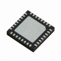
IR3622MPBF

IR3622MPBF

  • 厂商:

    IRF

  • 封装:

  • 描述:

    IR3622MPBF - HIGH FREQUENCY 2-PHASE, SINGLE OR DUAL OUTPUT SYNCHRONOUS STEP DOWN CONTROLLER WITH OUT...

  • 详情介绍
  • 数据手册
  • 价格&库存
IR3622MPBF 数据手册
Data Sheet No.PD94722 revA IR3622MPbF HIGH FREQUENCY 2-PHASE, SINGLE OR DUAL OUTPUT SYNCHRONOUS STEP DOWN CONTROLLER WITH OUTPUT TRACKING AND SEQUENCING Description Features • • • • • • • • • • • • • • • • • • Dual Synchronous Controller with 180o Out of Phase Operation Configurable to 2-Independent Outputs or Current Shared Single Output Output Voltage Tracking Power up / down Sequencing Current Sharing Using Inductor’s DCR +/-1% Accurate Reference Voltage Programmable Switching Frequency up 600kHz Programmable Over Current Protection Hiccup Current Limit Using MOSFET Rds(on) sensing Latched Overvoltage Protection Dual Programmable Soft-Starts Programmable Enable Input Pre-Bias Start-up Dual Power Good Outputs On Board Regulator External Frequency Synchronization Thermal Protection 32-Lead MLPQ Package The IR3622 IC integrates a dual synchronous Buck controller, providing a high performance and flexible solution. The IR3622 can be configured as 2-independent outputs or as current shared single output. The current share configuration is ideal for high current applications. The IR3622 enables output tracking and sequencing of multiple rails in either ratiometric or simultaneous fashion. The IR3622 features 180o out of phase operation which reduces the required input/output capacitance and results in lower number of capacitors. The switching frequency is programmable from 200kHz to 600kHz per phase using one external resistor. In addition, IR3622 also allows the switching frequency to be synchronized to an external clock signal. Other key features offered by this device include two independent programmable soft starts, two independent power good outputs, precision enable input, and under voltage lockout function. The current limit is provided by sensing the lower MOSFET's on-resistance for optimum cost and performance. The output voltages are monitored through dedicated pins to protect against open circuit, and enhance faster response to an overvoltage event. Applications • • • • • Embedded Telecom Systems Distributed Point of Load Power Architectures Computing Peripheral Voltage Regulators Graphics Cards General DC/DC Converters Vin Vo1 Vo1 Vo2 Rt Comp1 Comp2 IR3622 Vo2 HDrv1 OCSet1 LDrv1 PGnd1 Vin HDrv2 OCSet2 LDrv2 Vout2 Vout1 Ratiometric Powerup Ratiometric Powerdown SS1 / SD Vout1 SS2 / SD Seq Track Vo1 Vo2 Vo1 Vo2 Gnd PGnd2 Simultaneous Powerup Simultaneous Powerdown ORDERING INFORMATION PKG DESIG M M PACKAGE DESCRIPTION IR3622MPbF IR3622MTRPbF PIN PARTS PARTS COUNT PER TUBE PER REEL 32 73 ------32 -------3000 T&R ORIANTAION Fig A 03/15/07 www.irf.com IR3622MPbF ABSOLUTE MAXIMUM RATINGS (Voltages referenced to GND) Vcc, VcL Supply Voltage .....................................… -0.5V to 16V VcH1,VcH2 ……………………….………….……… -0.5V to 30V PGood1, PGood2 ………. .…………………………. -0.5V to 16V HDrv1, HDrv2 ………………………………………… -0.5V to 30V (-2V for 100ns) LDrv1, LDrv2 ………………………………………… -0.5V to 16V (-2V for 100ns) Gnd to PGnd ……………………………………….. +/- 0.3V Storage Temperature Range .................................. -65°C To 150°C Operating Junction Temperature Range ................ -40°C To 125°C ESD Classification ………………………………..… JEDEC, JESD22-A114 (1KV) Moisture Sensitivity Level ………………………….. JEDEC, Level 3 @ 260oC Caution: Stresses above those listed in “Absolute Maximum Rating” may cause permanent damage to the device. These are stress ratings only and function of the device at these or any other conditions beyond those indicated in the operational sections of the specifications is not implied. Exposure to “Absolute Maximum Rating” conditions for extended periods may affect device reliability. Package Information PG oo d1 Gn d VR Tra ck VO UT 3 EF Vc c 2 32 Rt VSEN2 Fb2 1 2 31 30 29 28 27 VP 26 VP 25 24 PGood2 23 Sync 22 VSEN1 3 Comp2 4 SS2/SD2/Mode 5 1 Pad 21 Fb1 20 Comp1 19 SS1/SD1 18 OCSet1 17 VcH1 OCSet2 6 VcH2 HDrv2 7 8 9 10 11 12 VcL 13 14 15 16 En ab le PG nd 2 LD rv2 www.irf.com *Exposed pad on underside is connected to a copper pad through vias for 4-layer PCB board design ΘJA = 36o C/W* ΘJC = 1o C/W LD rv1 PG nd 1 Se q HD rv1 2 IR3622MPbF Recommended Operating Conditions Symbol Vcc, VcL VcH1, VcH2 Fs Tj Definition Supply Voltage Supply Voltage Operating frequency Junction temperature Min 7.5 Converter Voltage + 5V 200 -40 Max 14.5 28 600 125 Units V V kHz o C Electrical Specifications Unless otherwise specified, these specification apply over Vcc=VcL=VcH1=VcH2=12V, 0oC> 1 - - - -(21) By replacing Zin and Zf according to figure 15, the transformer function can be expressed as: H (s ) = (1 + sR7C11 ) * [1 + sC10 (R6 + R8 )] 1 * sR6 (C11 + C12 ) ⎡ ⎛ C11 * C12 ⎞⎤ ⎢1 + sR7 ⎜ ⎜ C + C ⎟⎥ * (1 + sR8C10 ) ⎟ ⎝ 11 12 ⎠ ⎦ ⎣ Cross over frequency is expressed as: Vin 1 * Vosc 2π * Lo * Co Fo = R7 * C10 * www.irf.com 22 IR3622MPbF Based on the frequency of the zero generated by output capacitor and its ESR versus crossover frequency, the compensation type can be different. The table below shows the compensation types and location of crossover frequency. Compensator type TypII(PI) TypeIII(PID) Method A TypeIII(PID) Method B FESR vs. Fo Output capacitor Electrolytic , Tantalum Tantalum, ceramic Ceramic The following design rules will give a crossover frequency approximately one-sixth of the switching frequency. The higher the band width, the potentially faster the load transient response. The DC gain will be large enough to provide high DC-regulation accuracy (typically -5dB to -12dB). The phase margin should be greater than 45o for overall stability. R7 ≥ 2 ; R7 ≥ 0.67KΩ ; Select : R7 = 6.04KΩ gm FLC
IR3622MPBF
1. 物料型号: - 型号为IR3622MPbF,是一款32引脚的MLPQ封装的集成电路。

2. 器件简介: - IR3622是一款双相同步降压控制器,提供高达600kHz的可编程开关频率,支持独立双输出或电流共享的单输出配置,适用于高电流应用。

3. 引脚分配: - 引脚1 (Rt) 用于设置开关频率。 - 引脚2至32包括各种功能引脚,如电压监控、反馈、使能、同步、功率好输出等。

4. 参数特性: - 供电电压(Vcc, VcL):7.5V至14.5V。 - 工作频率(Fs):200kHz至600kHz。 - 接点温度(Tj):-40℃至125℃。

5. 功能详解: - 支持双相180度错相操作,降低输入/输出电容需求。 - 可配置的软启动和电源好输出。 - 支持外部频率同步。 - 热保护和过压保护功能。

6. 应用信息: - 适用于嵌入式电信系统、分布式负载点电源架构、计算外设电压调节器、图形卡等。

7. 封装信息: - 采用32引脚的MLPQ封装,具体封装设计参数包括标记区域、引脚间距等。
IR3622MPBF 价格&库存

很抱歉,暂时无法提供与“IR3622MPBF”相匹配的价格&库存,您可以联系我们找货

免费人工找货