Data Sheet No.PD94717 revF
IR3623MPbF
HIGH FREQUENCY 2-PHASE, SINGLE OR DUAL OUTPUT SYNCHRONOUS STEP DOWN CONTROLLER WITH OUTPUT TRACKING AND SEQUENCING Description Features
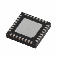
• • • • • • • • • • • • • • • • • • • • • • • Dual Synchronous Controller with 180o Out of Phase Operation Configurable to 2-Independent Outputs or Current Share Single Output Output Voltage Tracking Power up /down Sequencing Current Sharing Using Inductor’s DCR +/-1% Accurate Reference Voltage Programmable Switching Frequency up 1200kHz Programmable Over Current Protection Hiccup Current Limit Using MOSFET RDS(on) sensing Latched Overvoltage Protection Dual Programmable Soft-Starts Enable Pre-Bias Start-up Dual Power Good Outputs On Board Regulator External Frequency Synchronization Thermal Protection 32-Lead MLPQ Package Embedded Telecom Systems Distributed Point of Load Power Architectures Computing Peripheral Voltage Regulator Graphics Card General DC/DC Converters The IR3623 IC is a high performance Synchronous Buck PWM Controller that can be configured for two independent outputs or as a current sharing single output. Since the IC does not contain integrated MOSFET drivers it is ideal for controlling iPOWIRTM integrated power stage modules such as the iP2005 series of products. IR3623 enables output tracking and sequencing of multiple rails in either ratiometric or simultaneous fashion. The IR3623 features 180o out of phase operation which reduces the required input/output capacitance. The switching frequency is programmable from 200kHz to 1200kHz per phase by use of an external resistor or the switching frequency can be synchronized to an external clock signal. Other key features offered by the IR3623 include; two independent programmable soft starts, two independent power good outputs, precision enable input and under voltage lockout. The current limit is provided by sensing the low side MOSFET's on-resistance for optimum cost and performance. The output voltages are monitored through dedicated pins to protect against open circuit and to improve response time to an overvoltage event.
Applications
Vo1 Vo2
Vo1 Vo2
Ratiometric Powerup
Ratiometric Powerdown
Vo1 Vo2
Vo1 Vo2
Simultaneous Powerup
Simultaneous Powerdown
Fig. 1: Power Up /Down Sequencing
ORDERING INFORMATION
PKG DESIG M M PACKAGE DESCRIPTION IR3623MPbF IR3623MTRPbF PIN COUNT 32 32 PARTS PARTS PER TUBE PER REEL 73 -------------3000 T&R ORIANTAION
Fig A
www.irf.com
�IR3623MPbF
ABSOLUTE MAXIMUM RATINGS
(Voltages referenced to GND)
•Vcc Supply Voltage ...............................................… -0.5V to 16V •PWM1, PWM2 …………………….………….……….. -0.5V to 16V •PGood ………. ……………………………………….. -0.5V to 16V •Gnd to SGnd ………………………………………… +/- 0.3V •Storage Temperature Range .................................... -65°C To 150°C •Operating Junction Temperature Range .................. -40°C To 125°C •ESD Classification …………………………………… JEDEC, JESD22-A114
Caution: Stresses above those listed in “Absolute Maximum Rating” may cause permanent damage to the
device. These are stress ratings only and function of the device at these or any other conditions beyond those indicated in the operational sections of the specifications is not implied. Exposure to “Absolute Maximum Rating” conditions for extended periods may affect device reliability.
Package Information
5V _sn s En ab le Rt
Gn d SG nd VR
EF
2
32 PGood1 1 PGood2 2 Track2 3 VSEN2 4 OVP_Output 5
31
30
29
28 27
VP
26
25 24 Seq 23 Sync 22 Track1
VP
1
Pad
21 VSEN1 20 19 OCGnd Fb1
Fb2 6 Comp2 7 SS2/SD2/Mode 8 9 10 11 12
C
18 Comp1 17 SS1/SD1 13
UT 3
14
15
16
OC Se t2 Ph _E n2 PW M2 VC
ΘJA = 36o C/W ΘJC = 1o C/W
*Exposed pad on underside is connected to a copper pad through vias for 4-layer PCB board design
www.irf.com
PW M1 Ph _E n1 OC Se t1
VO
2
�IR3623MPbF
Recommended Operating Conditions
Symbol
Vcc Fs Tj
Definition
Supply Voltage Operating frequency Junction temperature
Min
8.5 200 -40
Max
14.5 1200 125
Units
V kHz o C
Electrical Specifications
Unless otherwise specified, these specification apply over Vcc=12V, 0oC 1
- - - -(21)
By replacing Zin and Zf according to figure 15, the transformer function can be expressed as:
(1 + sR7C11 ) * [1 + sC10 (R6 + R8 )] 1 * H (s ) = sR6 (C11 + C12 ) ⎡ ⎛ C11 * C12 ⎞⎤ ⎢1 + sR7 ⎜ ⎜ C + C ⎟⎥ * (1 + sR8C10 ) ⎟ ⎝ 11 12 ⎠ ⎦ ⎣
www.irf.com
Cross over frequency is expressed as:
Fo = R7 * C10 * Vin 1 * Vosc 2π * Lo * Co
20
�IR3623MPbF
Based on the frequency of the zero generated by output capacitor and its ESR versus crossover frequency, the compensation type can be different. The table below shows the compensation types and location of crossover frequency.
Compensator type TypII(PI)
FESR vs. Fo
Output capacitor Electrolytic , Tantalum Tantalum, ceramic Ceramic
FLC
很抱歉,暂时无法提供与“IR3623MTRPBF”相匹配的价格&库存,您可以联系我们找货
免费人工找货