Data Sheet No PD94725
IR3628MPbF
HIGH FREQUENCY SYNCHRONOUS PWM BUCK CONTROLLER
Features
• • • • • • • • • • • • • • • • • Internal 600kHz Oscillator Operates with Single 5V or 12V Supply Programmable Over Current Protection Hiccup Current Limit Using MOSFET RDS(on) sensing Tracking for memory application Precision Reference Voltage (0.6V) Programmable Soft-Start Pre-Bias Start-up Thermal Protection 12-Lead 3x4mm MLPD Package DDR Application Storage Systems Embedded Telecom Systems Distributed Point of Load Power Architectures Computing Peripheral Voltage Regulator Graphics Card General DC/DC Converters
Description
The IR3628 is a PWM controller designed for high performance synchronous Buck DC/DC applications. The IR3628 drives a pair of external N-MOSFETs using a fixed 600kHz switching frequency allowing the use of small external components. The output voltage can be precisely regulated using the internal 0.6V reference voltage for low voltage applications. IR3628 provides an efficient solution for high-speed bandwidth data bus which requires a particular tracking scheme for best performance using the uncommitted error amplifier. Protection such as Pre-Bias startup, hiccup current limit and thermal shutdown are provided to give required system level security in the event of fault conditions.
Applications
Fig. 1: Typical application Circuit
ORDERING INFORMATION
PKG DESIG M M PACKAGE DESCRIPTION IR3628MPBF IR3628MTRPBF PIN PARTS PARTS COUNT PER TUBE PER REEL 12 122 ------12 -------3000 T&R ORIANTAION
Figure A
08/10/2007
�IR3628MPbF
ABSOLUTE MAXIMUM RATINGS
(Voltages referenced to GND)
• • • • • • • • •
Vcc Supply Voltage ................................................… -0.5V to 16V Vc Supply Voltage …………………………………….. -0.5V to 30V Vref, Vp, Fb, Comp, SS …………..………………….. -0.3V to 3.5V OCset ………………………………………………… 10mA AGnd to PGnd ………………………………….…….. -0.3V to +0.3V Storage Temperature Range ..................................... -65°C To 150°C Operating Junction Temperature Range ................... -40°C To 150°C ESD Classification …………………………………..… JEDEC, JESD22-A114 Moisture Sensitivity Level ……………………………. JEDEC Level 2 @ 260oC
Caution: Stresses beyond those listed under “Absolute Maximum Rating” may cause permanent damage to the device. These are stress ratings only and functional operation of the device at these or any other conditions beyond those indicated in the operational sections of the specifications is not implied. Exposure to “Absolute Maximum Rating” conditions for extended periods may affect device reliability.
Package Information
Vref VCC LDrv PGnd HDrv VC
1 2 3 4 5 6
12 11 10 9 8 7
OCSet SS/SD Gnd Comp Fb Vp
Exposed Pad
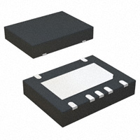
12-Lead MLPD, 3x4mm
ΘJA = 30o C/W * ΘJC = 2o C/W
*Exposed pad on underside is connected to a copper pad through vias for 4-layer PCB board design
08/10/2007
2
�IR3628MPbF
Block Diagram
Fig. 2: Simplified block diagram of the IR3628
08/10/2007
3
�IR3628MPbF
Pin Description
Pin Name
1 2 3 4 5 6 7 8 9 10 11 Vref Vcc LDrv PGnd HDrv Vc Vp Fb Comp Gnd SS/SD
Description
External reference voltage. Drive capability for this pin is 2uA. This pin provides power for the internal blocks of the IC as well as powers the low side driver. A minimum of 0.1uF, high frequency capacitor must be connected from this pin to power ground. Output driver for low side MOSFET Power Ground. This pin serves as a separate ground for the MOSFET drivers and should be connected to the system’s power ground plane. Output driver for high side MOSFET This pin powers the high side driver and must be connected to a voltage higher than bus voltage. A minimum of 0.1uF, high frequency capacitor must be connected from this pin to power ground. Non inverting input of error amplifier, this pin can be used for tracking application. Inverting input to the error amplifier. This pin is connected directly to the output of the regulator via resistor divider to set the output voltage and provide feedback to the error amplifier. Output of error amplifier. An external resistor and capacitor network is typically connected from this pin to ground to provide loop compensation. Signal ground for internal reference and control circuitry. Soft start / shutdown. This pin provides user programmable soft-start function. Connect an external capacitor from this pin to ground to set the start up time of the output voltage. The converter can be shutdown by pulling this pin below 0.3V. Current limit set point. A resistor from this pin to drain of low side MOSFET will set the current limit threshold.
12
OCSet
08/10/2007
4
�IR3628MPbF
Recommended Operating Conditions
Symbol Vcc Vc Tj* Definition Supply Voltage Supply Voltage Junction Temperature Min 4.5 Converter voltage + 5 -40 Max 14 28 125 Units V V o C
*The junction Temperature for 5V application is 0oC-125oC
Electrical Specifications
Unless otherwise specified, these specification apply over Vcc=Vc=12V, 0oC
很抱歉,暂时无法提供与“IR3628MTRPBF”相匹配的价格&库存,您可以联系我们找货
免费人工找货