PD-94968
IRF1404PbF
Advanced Process Technology l Ultra Low On-Resistance l Dynamic dv/dt Rating l 175°C Operating Temperature l Fast Switching l Fully Avalanche Rated l Automotive Qualified (Q101) l Lead-Free Description
l
HEXFET® Power MOSFET
D
VDSS = 40V RDS(on) = 0.004Ω
G S
ID = 202A
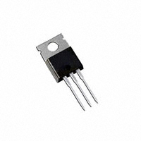
Seventh Generation HEXFET® Power MOSFETs from International Rectifier utilize advanced processing techniques to achieve extremely low on-resistance per silicon area. This benefit, combined with the fast switching speed and ruggedized device design that HEXFET power MOSFETs are well known for, provides the designer with an extremely efficient and reliable device for use in a wide variety of applications including automotive. The TO-220 package is universally preferred for all automotive-commercial-industrial applications at power dissipation levels to approximately 50 watts. The low thermal resistance and low package cost of the TO-220 contribute to its wide acceptance throughout the industry.
TO-220AB
Absolute Maximum Ratings
ID @ TC = 25°C ID @ TC = 100°C IDM PD @TC = 25°C VGS EAS IAR EAR dv/dt TJ TSTG
Parameter
Continuous Drain Current, VGS @ 10V Continuous Drain Current, VGS @ 10V Pulsed Drain Current Power Dissipation Linear Derating Factor Gate-to-Source Voltage Single Pulse Avalanche Energy Avalanche Current Repetitive Avalanche Energy Peak Diode Recovery dv/dt Operating Junction and Storage Temperature Range Soldering Temperature, for 10 seconds Mounting Torque, 6-32 or M3 screw
Max.
202 143 808 333 2.2 ± 20 620 See Fig.12a, 12b, 15, 16 1.5 -55 to + 175 -55 to + 175 300 (1.6mm from case ) 10 lbf•in (1.1N•m)
Units
A W W/°C V mJ A mJ V/ns °C
Thermal Resistance
Parameter
RθJC RθCS RθJA Junction-to-Case Case-to-Sink, Flat, Greased Surface Junction-to-Ambient
Typ.
––– 0.50 –––
Max.
0.45 ––– 62
Units
°C/W
www.irf.com
1
02/02/04
�IRF1404PbF
Electrical Characteristics @ TJ = 25°C (unless otherwise specified)
V(BR)DSS
∆V(BR)DSS/∆TJ
RDS(on) VGS(th) gfs IDSS IGSS Qg Qgs Qgd td(on) tr td(off) tf LD LS Ciss Coss Crss Coss Coss Coss eff.
Parameter Drain-to-Source Breakdown Voltage Breakdown Voltage Temp. Coefficient Static Drain-to-Source On-Resistance Gate Threshold Voltage Forward Transconductance Drain-to-Source Leakage Current Gate-to-Source Forward Leakage Gate-to-Source Reverse Leakage Total Gate Charge Gate-to-Source Charge Gate-to-Drain ("Miller") Charge Turn-On Delay Time Rise Time Turn-Off Delay Time Fall Time Internal Drain Inductance Internal Source Inductance Input Capacitance Output Capacitance Reverse Transfer Capacitance Output Capacitance Output Capacitance Effective Output Capacitance
Min. 40 ––– ––– 2.0 76 ––– ––– ––– ––– ––– ––– ––– ––– ––– ––– ––– ––– ––– ––– ––– ––– ––– ––– –––
Typ. Max. Units Conditions ––– ––– V VGS = 0V, ID = 250µA 0.039 ––– V/°C Reference to 25°C, ID = 1mA 0.0035 0.004 Ω VGS = 10V, ID = 121A ––– 4.0 V VDS = 10V, ID = 250µA ––– ––– S VDS = 25V, ID = 121A ––– 20 VDS = 40V, VGS = 0V µA ––– 250 VDS = 32V, VGS = 0V, TJ = 150°C ––– 200 VGS = 20V nA ––– -200 VGS = -20V 131 196 ID = 121A 36 ––– nC VDS = 32V 37 56 VGS = 10V 17 ––– VDD = 20V 190 ––– ID = 121A ns 46 ––– RG = 2.5Ω 33 ––– RD = 0.2Ω D Between lead, 4.5 ––– 6mm (0.25in.) nH G from package 7.5 ––– and center of die contact S 5669 ––– VGS = 0V 1659 ––– pF VDS = 25V 223 ––– ƒ = 1.0MHz, See Fig. 5 6205 ––– VGS = 0V, VDS = 1.0V, ƒ = 1.0MHz 1467 ––– VGS = 0V, VDS = 32V, ƒ = 1.0MHz 2249 ––– VGS = 0V, VDS = 0V to 32V
Source-Drain Ratings and Characteristics
IS
ISM
VSD trr Qrr ton Notes:
Parameter Continuous Source Current (Body Diode) Pulsed Source Current (Body Diode) Diode Forward Voltage Reverse Recovery Time Reverse RecoveryCharge Forward Turn-On Time
Min. Typ. Max. Units
Conditions D MOSFET symbol ––– ––– 202 showing the A G integral reverse ––– ––– 808 S p-n junction diode. ––– ––– 1.5 V TJ = 25°C, IS = 121A, VGS = 0V ––– 78 117 ns TJ = 25°C, IF = 121A ––– 163 245 nC di/dt = 100A/µs Intrinsic turn-on time is negligible (turn-on is dominated by LS+LD)
Repetitive rating; pulse width limited by Starting TJ = 25°C, L = 85µH
RG = 25Ω, IAS = 121A. (See Figure 12)
max. junction temperature. (See fig. 11)
Pulse width ≤ 400µs; duty cycle ≤ 2%.
Coss eff. is a fixed capacitance that gives the same charging time
as Coss while VDS is rising from 0 to 80% VDSS Calculated continuous current based on maximum allowable junction temperature. Package limitation current is 75A.
ISD ≤ 121A, di/dt ≤ 130A/µs, VDD ≤ V(BR)DSS,
TJ ≤ 175°C
2
www.irf.com
�IRF1404PbF
1000
I D , Drain-to-Source Current (A)
100
I D , Drain-to-Source Current (A)
VGS 15V 10V 8.0V 7.0V 6.0V 5.5V 5.0V BOTTOM 4.5V TOP
1000
100
VGS 15V 10V 8.0V 7.0V 6.0V 5.5V 5.0V BOTTOM4.5V TOP
4.5V
10
4.5V
10
1 0.1
20µs PULSE WIDTH TJ = 25 °C
1 10 100
1 0.1
20µs PULSE WIDTH TJ = 175 °C
1 10 100
VDS , Drain-to-Source Voltage (V)
VDS , Drain-to-Source Voltage (V)
Fig 1. Typical Output Characteristics
Fig 2. Typical Output Characteristics
TJ = 25 ° C TJ = 175 ° C
RDS(on) , Drain-to-Source On Resistance (Normalized)
1000
2.5
ID = 202A
I D , Drain-to-Source Current (A)
2.0
1.5
100
1.0
0.5
10
V DS= 25V 20µs PULSE WIDTH 4 5 6 7 8 9 10 11 12
0.0 -60 -40 -20 0
VGS = 10V
20 40 60 80 100 120 140 160 180
VGS , Gate-to-Source Voltage (V)
TJ , Junction Temperature ( ° C)
Fig 3. Typical Transfer Characteristics
Fig 4. Normalized On-Resistance Vs. Temperature
www.irf.com
3
�IRF1404PbF
10000
8000
C, Capacitance(pF)
Crss = C gd Coss = C + Cgd ds
VGS , Gate-to-Source Voltage (V)
VGS = 0V, f = 1 MHZ Ciss = C + Cgd, Cds SHORTED gs
20
ID = 121A
V DS= 32V V DS= 20V
16
6000
Ciss
12
4000
Coss
8
2000
Crss
0 1 10 100
4
0
FOR TEST CIRCUIT SEE FIGURE 13
0 50 100 150 200
VDS, Drain-to-Source Voltage (V)
QG , Total Gate Charge (nC)
Fig 5. Typical Capacitance Vs. Drain-to-Source Voltage
Fig 6. Typical Gate Charge Vs. Gate-to-Source Voltage
1000
10000
ISD , Reverse Drain Current (A)
TJ = 175 ° C
OPERATION IN THIS AREA LIMITED BY RDS(on)
ID , Drain Current (A)
100
1000 10us
10
100
100us 1ms
TJ = 25 ° C
1
10
10ms
0.1 0.0
V GS = 0 V
0.5 1.0 1.5 2.0 2.5 3.0 3.5
1
TC = 25 °C TJ = 175 °C Single Pulse
1 10 100
VSD ,Source-to-Drain Voltage (V)
VDS , Drain-to-Source Voltage (V)
Fig 7. Typical Source-Drain Diode Forward Voltage
Fig 8. Maximum Safe Operating Area
4
www.irf.com
�IRF1404PbF
220 200 180
LIMITED BY PACKAGE
VGS RG 10V
VDS
RD
D.U.T.
+
ID , Drain Current (A)
160 140 120 100 80 60 40 20 0 25 50 75 100 125 150 175
-V DD
Pulse Width ≤ 1 µs Duty Factor ≤ 0.1 %
Fig 10a. Switching Time Test Circuit
VDS 90%
TC , Case Temperature ( °C)
Fig 9. Maximum Drain Current Vs. Case Temperature
10% VGS
td(on) tr t d(off) tf
Fig 10b. Switching Time Waveforms
1
Thermal Response (Z thJC )
D = 0.50 0.1 0.20 0.10 0.05 0.02 0.01 SINGLE PULSE (THERMAL RESPONSE) PDM t1 t2 Notes: 1. Duty factor D = t 1 / t 2 2. Peak TJ = P DM x Z thJC + TC 0.0001 0.001 0.01 0.1
0.01
0.001 0.00001
t1 , Rectangular Pulse Duration (sec)
Fig 11. Maximum Effective Transient Thermal Impedance, Junction-to-Case
www.irf.com
5
�IRF1404PbF
15V
EAS , Single Pulse Avalanche Energy (mJ)
1500
VDS
L
DRIVER
1200
ID 49A 101A BOTTOM 121A TOP
RG
20V
D.U.T
IAS tp
+ V - DD
900
A
0.01Ω
600
Fig 12a. Unclamped Inductive Test Circuit
V(BR)DSS tp
300
0
25
Starting TJ , Junction Temperature ( ° C)
50
75
100
125
150
175
I AS
Fig 12b. Unclamped Inductive Waveforms
QG
Fig 12c. Maximum Avalanche Energy Vs. Drain Current
10 V
QGS
QGD
-VGS(th) Gate threshold Voltage (V)
4.0
VG
3.0
Charge
ID = -250µA
Fig 13a. Basic Gate Charge Waveform
Current Regulator Same Type as D.U.T.
2.0
50KΩ 12V .2µF .3µF
D.U.T. VGS
3mA
+ V - DS
1.0 -75 -50 -25 0 25 50 75 100 125 150
T J , Temperature ( °C )
IG ID
Current Sampling Resistors
Fig 14. Threshold Voltage Vs. Temperature
Fig 13b. Gate Charge Test Circuit
6
www.irf.com
�IRF1404PbF
1000
Duty Cycle = Single Pulse
Avalanche Current (A)
0.01
100
0.05 0.10
10
Allowed avalanche Current vs avalanche pulsewidth, tav assuming ∆ Tj = 25°C due to avalanche losses
1 1.0E-08 1.0E-07 1.0E-06 1.0E-05 1.0E-04 1.0E-03 1.0E-02 1.0E-01
tav (sec)
Fig 15. Typical Avalanche Current Vs.Pulsewidth
400 350
EAR , Avalanche Energy (mJ)
300 250 200 150 100 50 0 25 50
TOP Single Pulse BOTTOM 10% Duty Cycle ID = 121A
75
100
125
150
Starting T J , Junction Temperature (°C)
Notes on Repetitive Avalanche Curves , Figures 15, 16: (For further info, see AN-1005 at www.irf.com) 1. Avalanche failures assumption: Purely a thermal phenomenon and failure occurs at a temperature far in excess of Tjmax. This is validated for every part type. 2. Safe operation in Avalanche is allowed as long asTjmax is not exceeded. 3. Equation below based on circuit and waveforms shown in Figures 12a, 12b. 4. PD (ave) = Average power dissipation per single avalanche pulse. 5. BV = Rated breakdown voltage (1.3 factor accounts for voltage increase during avalanche). 6. Iav = Allowable avalanche current. 7. ∆T = Allowable rise in junction temperature, not to exceed Tjmax (assumed as 25°C in Figure 15, 16). tav = Average time in avalanche. 175 D = Duty cycle in avalanche = t av ·f ZthJC(D, tav) = Transient thermal resistance, see figure 11) PD (ave) = 1/2 ( 1.3·BV·Iav) = DT/ ZthJC Iav = 2DT/ [1.3·BV·Zth] EAS (AR) = PD (ave)·tav
Fig 16. Maximum Avalanche Energy Vs. Temperature
www.irf.com
7
�IRF1404PbF
Peak Diode Recovery dv/dt Test Circuit
D.U.T
+
+
Circuit Layout Considerations • Low Stray Inductance • Ground Plane • Low Leakage Inductance Current Transformer
-
+
RG • • • • dv/dt controlled by RG Driver same type as D.U.T. ISD controlled by Duty Factor "D" D.U.T. - Device Under Test
+ VDD
Driver Gate Drive P.W. Period D=
P.W. Period VGS=10V
*
D.U.T. ISD Waveform Reverse Recovery Current Body Diode Forward Current di/dt D.U.T. VDS Waveform Diode Recovery dv/dt
VDD
Re-Applied Voltage Inductor Curent
Body Diode
Forward Drop
Ripple ≤ 5%
ISD
* VGS = 5V for Logic Level Devices Fig 17. For N-channel HEXFET® Power MOSFETs
8
www.irf.com
�IRF1404PbF
TO-220AB Package Outline
2.87 (.113) 2.62 (.103) 10.54 (.415) 10.29 (.405) 3.78 (.149) 3.54 (.139) -A6.47 (.255) 6.10 (.240)
Dimensions are shown in millimeters (inches)
-B4.69 (.185) 4.20 (.165) 1.32 (.052) 1.22 (.048)
4 15.24 (.600) 14.84 (.584)
1.15 (.045) MIN 1 2 3
LEAD ASSIGNMENTS IGBTs, CoPACK 1 - GATE 21- GATE DRAIN 1- GATE 32- DRAINSOURCE 2- COLLECTOR 3- SOURCE 3- EMITTER 4 - DRAIN
LEAD ASSIGNMENTS
HEXFET
14.09 (.555) 13.47 (.530)
4- DRAIN
4.06 (.160) 3.55 (.140)
4- COLLECTOR
3X 3X 1.40 (.055) 1.15 (.045)
0.93 (.037) 0.69 (.027) M BAM
3X
0.55 (.022) 0.46 (.018)
0.36 (.014)
2.54 (.100) 2X NOTES: 1 DIMENSIONING & TOLERANCING PER ANSI Y14.5M, 1982. 2 CONTROLLING DIMENSION : INCH
2.92 (.115) 2.64 (.104)
3 OUTLINE CONFORMS TO JEDEC OUTLINE TO-220AB. 4 HEATSINK & LEAD MEASUREMENTS DO NOT INCLUDE BURRS.
TO-220AB Part Marking Information
E XAMPL E : T HIS IS AN IR F 1010 LOT CODE 1789 AS S E MB L E D ON WW 19, 1997 IN T H E AS S E MB LY L INE "C" INT E R NAT IONAL R E CT IF IE R L OGO AS S E MB L Y LOT CODE PAR T NU MB E R
Note: "P" in assembly line position indicates "Lead-Free"
DAT E CODE YE AR 7 = 1997 WE E K 19 L INE C
TO-220AB package is not recommended for Surface Mount Application.
Data and specifications subject to change without notice. This product has been designed and qualified for the automotive [Q101] market. Qualification Standards can be found on IR’s Web site.
IR WORLD HEADQUARTERS: 233 Kansas St., El Segundo, California 90245, USA Tel: (310) 252-7105 TAC Fax: (310) 252-7903 Visit us at www.irf.com for sales contact information.02/04
www.irf.com
9
�Note: For the most current drawings please refer to the IR website at: http://www.irf.com/package/
�