SMPS MOSFET
PD-95114
IRF730AS/LPbF
HEXFET® Power MOSFET
Applications l Switch Mode Power Supply (SMPS) l Uninterruptable Power Supply l High speed power switching l Lead-Free Benefits l Low Gate Charge Qg results in Simple Drive Requirement l Improved Gate, Avalanche and dynamic dv/dt Ruggedness l Fully Characterized Capacitance and Avalanche Voltage and Current l Effective Coss Specified (See AN1001)
VDSS
400V
Rds(on) max
1.0Ω
ID
5.5A
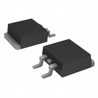
D 2 Pak
TO-262
Absolute Maximum Ratings
Parameter
ID @ TC = 25°C ID @ TC = 100°C IDM PD @TC = 25°C VGS dv/dt TJ TSTG Continuous Drain Current, VGS @ 10V Continuous Drain Current, VGS @ 10V Pulsed Drain Current Power Dissipation Linear Derating Factor Gate-to-Source Voltage Peak Diode Recovery dv/dt Operating Junction and Storage Temperature Range Soldering Temperature, for 10 seconds
Max.
5.5 3.5 22 74 0.6 ± 30 4.6 -55 to + 150 300 (1.6mm from case )
Units
A W W/°C V V/ns °C
Typical SMPS Topologies:
l l
Single Transistor Flyback Xfmr. Reset Single Transistor Forward Xfmr. Reset (Both US Line input only).
through are on page 10
Notes
www.irf.com
1
3/16/04
�IRF730AS/LPbF
V(BR)DSS
Static @ TJ = 25°C (unless otherwise specified)
Parameter Drain-to-Source Breakdown Voltage ∆V(BR)DSS/∆TJ Breakdown Voltage Temp. Coefficient RDS(on) Static Drain-to-Source On-Resistance VGS(th) Gate Threshold Voltage IDSS IGSS Drain-to-Source Leakage Current Gate-to-Source Forward Leakage Gate-to-Source Reverse Leakage Min. Typ. Max. Units Conditions 400 ––– ––– V VGS = 0V, ID = 250µA ––– 0.5 ––– V/°C Reference to 25°C, ID = 1mA ––– ––– 1.0 Ω VGS = 10V, ID = 3.3A 2.0 ––– 4.5 V VDS = VGS, ID = 250µA ––– ––– 25 VDS = 400V, VGS = 0V µA ––– ––– 250 VDS = 320V, VGS = 0V, TJ = 125°C ––– ––– 100 VGS = 30V nA ––– ––– -100 VGS = -30V
Dynamic @ TJ = 25°C (unless otherwise specified)
gfs Qg Qgs Qgd td(on) tr td(off) tf Ciss Coss Crss Coss Coss Coss eff. Parameter Forward Transconductance Total Gate Charge Gate-to-Source Charge Gate-to-Drain ("Miller") Charge Turn-On Delay Time Rise Time Turn-Off Delay Time Fall Time Input Capacitance Output Capacitance Reverse Transfer Capacitance Output Capacitance Output Capacitance Effective Output Capacitance Min. 3.1 ––– ––– ––– ––– ––– ––– ––– ––– ––– ––– ––– ––– ––– Typ. ––– ––– ––– ––– 10 22 20 16 600 103 4.0 890 30 45 Max. Units Conditions ––– S VDS = 50V, ID = 3.3A 22 ID = 3.5A 5.8 nC VDS = 320V 9.3 VGS = 10V, See Fig. 6 and 13 ––– VDD = 200V ––– ID = 3.5A ns ––– R G = 12Ω ––– R D = 57Ω,See Fig. 10 ––– VGS = 0V ––– VDS = 25V ––– pF ƒ = 1.0MHz, See Fig. 5 ––– VGS = 0V, VDS = 1.0V, ƒ = 1.0MHz ––– VGS = 0V, VDS = 320V, ƒ = 1.0MHz ––– VGS = 0V, VDS = 0V to 320V
Avalanche Characteristics
Parameter
EAS IAR EAR Single Pulse Avalanche Energy Avalanche Current Repetitive Avalanche Energy
Typ.
––– ––– –––
Max.
290 5.5 7.4
Units
mJ A mJ
Thermal Resistance
Parameter
RθJC RθJA Junction-to-Case Junction-to-Ambient ( PCB Mounted, steady-state)*
Typ.
––– –––
Max.
1.7 40
Units
°C/W
Diode Characteristics
IS
ISM
VSD trr Qrr ton
Parameter Continuous Source Current (Body Diode) Pulsed Source Current (Body Diode) Diode Forward Voltage Reverse Recovery Time Reverse RecoveryCharge Forward Turn-On Time
Min. Typ. Max. Units
Conditions D MOSFET symbol ––– ––– 5.5 showing the A G integral reverse ––– ––– 22 S p-n junction diode. ––– ––– 1.6 V TJ = 25°C, IS = 5.5A, VGS = 0V ––– 370 550 ns TJ = 25°C, IF = 3.5A ––– 1.6 2.4 µC di/dt = 100A/µs Intrinsic turn-on time is negligible (turn-on is dominated by LS+LD)
2
www.irf.com
�IRF730AS/LPbF
100
VGS 15V 10V 8.0V 7.0V 6.0V 5.5V 5.0V BOTTOM 4.5V TOP
100
I D , Drain-to-Source Current (A)
I D , Drain-to-Source Current (A)
10
10
VGS 15V 10V 8.0V 7.0V 6.0V 5.5V 5.0V BOTTOM 4.5V TOP
1
1
4.5V
0.1
0.1
4.5V
20µs PULSE WIDTH TJ = 25 °C
1 10 100
0.01 0.1
VDS , Drain-to-Source Voltage (V)
0.01 0.1
20µs PULSE WIDTH TJ = 150 °C
1 10 100
VDS , Drain-to-Source Voltage (V)
Fig 1. Typical Output Characteristics
Fig 2. Typical Output Characteristics
100
2.5
RDS(on) , Drain-to-Source On Resistance (Normalized)
5.9A ID = 5.5
I D , Drain-to-Source Current (A)
2.0
10
TJ = 150 ° C
1.5
1
TJ = 25 ° C
1.0
0.5
0.1 4.0
V DS = 50V 20µs PULSE WIDTH 5.0 6.0 7.0 8.0 9.0 10.0
VGS , Gate-to-Source Voltage (V)
0.0 -60 -40 -20
VGS = 10V
0 20 40 60 80 100 120 140 160
TJ , Junction Temperature ( °C)
Fig 3. Typical Transfer Characteristics
Fig 4. Normalized On-Resistance Vs. Temperature
www.irf.com
3
�IRF730AS/LPbF
100000
20
VGS , Gate-to-Source Voltage (V)
10000
VGS = 0V, f = 1 MHZ Ciss = C + Cgd, C gs ds SHORTED Crss = C gd Coss = C + C ds gd
ID =5.5 5.9A
16
VDS = 320V VDS = 200V VDS = 80V
C, Capacitance(pF)
1000
12
Ciss Coss
100
8
10
4
Crss
1 1 10 100 1000
0 0 5 10
FOR TEST CIRCUIT SEE FIGURE 13
15 20 25
QG , Total Gate Charge (nC)
VDS, Drain-to-Source Voltage (V)
Fig 5. Typical Capacitance Vs. Drain-to-Source Voltage
Fig 6. Typical Gate Charge Vs. Gate-to-Source Voltage
100
100
ISD , Reverse Drain Current (A)
OPERATION IN THIS AREA LIMITED BY RDS(on)
10us
10
TJ = 150 ° C
I D , Drain Current (A)
10 100us
1ms 1 10ms
1
TJ = 25 ° C
0.1 0.4
V GS = 0 V
0.6 0.8 1.0 1.2
0.1
TC = 25 °C TJ = 150 °C Single Pulse
10 100 1000
VSD ,Source-to-Drain Voltage (V)
VDS , Drain-to-Source Voltage (V)
Fig 7. Typical Source-Drain Diode Forward Voltage
Fig 8. Maximum Safe Operating Area
4
www.irf.com
�IRF730AS/LPbF
6.0
V DS VGS RG
RD
5.0
D.U.T.
+
ID , Drain Current (A)
4.0
- VDD
10V
3.0
Pulse Width ≤ 1 µs Duty Factor ≤ 0.1 %
2.0
Fig 10a. Switching Time Test Circuit
VDS 90%
1.0
0.0
25
50
75
100
125
150
TC , Case Temperature ( °C)
Fig 9. Maximum Drain Current Vs. Case Temperature
10% VGS
td(on) tr t d(off) tf
Fig 10b. Switching Time Waveforms
10
Thermal Response (Z thJC )
1 D = 0.50 0.20 0.10 0.1 0.05 0.02 0.01 PDM t1 SINGLE PULSE (THERMAL RESPONSE) t2 Notes: 1. Duty factor D = t 1 / t 2 2. Peak T J = P DM x Z thJC + TC 0.001 0.01 0.1 1
0.01 0.00001
0.0001
t1 , Rectangular Pulse Duration (sec)
Fig 11. Maximum Effective Transient Thermal Impedance, Junction-to-Case
www.irf.com
5
�IRF730AS/LPbF
EAS , Single Pulse Avalanche Energy (mJ)
15V
700 600 500 400 300 200 100 0
TOP BOTTOM
VDS
L
DRIVER
ID 2.5A 3.5A 5.5A
RG
20V
D.U.T
IAS tp
+ V - DD
A
0.01Ω
Fig 12a. Unclamped Inductive Test Circuit
V(BR)DSS tp
25
Starting TJ , Junction Temperature ( °C)
50
75
100
125
150
I AS
Fig 12b. Unclamped Inductive Waveforms
QG
610 600 590 580 570 560 550 540 0.0
3mA
Fig 12c. Maximum Avalanche Energy Vs. Drain Current
10 V
VG
Charge
Fig 13a. Basic Gate Charge Waveform
Current Regulator Same Type as D.U.T.
50KΩ 12V .2µF .3µF
D.U.T. VGS
+ V - DS
V DSav , Avalanche Voltage ( V )
QGS
QGD
1.0
2.0
3.0
4.0
5.0
6.0
IAV , Avalanche Current ( A)
IG ID
Current Sampling Resistors
Fig 13b. Gate Charge Test Circuit
Fig 12d. Typical Drain-to-Source Voltage Vs. Avalanche Current
6
www.irf.com
�IRF730AS/LPbF
Peak Diode Recovery dv/dt Test Circuit
D.U.T
+
+
Circuit Layout Considerations • Low Stray Inductance • Ground Plane • Low Leakage Inductance Current Transformer
-
+
RG • • • • dv/dt controlled by RG Driver same type as D.U.T. ISD controlled by Duty Factor "D" D.U.T. - Device Under Test
+ VDD
Driver Gate Drive P.W. Period D=
P.W. Period VGS=10V
*
D.U.T. ISD Waveform Reverse Recovery Current Body Diode Forward Current di/dt D.U.T. VDS Waveform Diode Recovery dv/dt
VDD
Re-Applied Voltage Inductor Curent
Body Diode
Forward Drop
Ripple ≤ 5%
ISD
* VGS = 5V for Logic Level Devices Fig 14. For N-Channel HEXFETS
www.irf.com
7
�IRF730AS/LPbF
Dimensions are shown in millimeters (inches)
D2Pak Package Outline
D2Pak Part Marking Information (Lead-Free)
T H IS IS AN IR F 5 3 0 S W IT H L OT CODE 80 2 4 AS S E M B L E D ON W W 0 2, 20 00 IN T H E AS S E M B L Y L IN E "L " N ote: "P " in as s em bly lin e po s itio n in dicates "L ead-F r ee" IN T E R N AT IO N AL R E C T IF IE R L OGO AS S E M B L Y L O T CO D E P AR T N U M B E R F 5 30 S D AT E C O D E Y E AR 0 = 2 0 0 0 W E E K 02 L IN E L
OR
IN T E R N AT IO N AL R E C T IF IE R L O GO AS S E M B L Y L OT COD E P AR T N U M B E R F 530S D AT E CO D E P = D E S IG N AT E S L E AD -F R E E P R O D U C T (O P T IO N AL ) Y E AR 0 = 2 0 0 0 W E E K 02 A = AS S E M B L Y S IT E CO D E
8
www.irf.com
�IRF730AS/LPbF
TO-262 Package Outline
IGBT 1- GATE 2- COLLECTOR 3- EMITTER
TO-262 Part Marking Information
EXAMPLE: T HIS IS AN IRL3103L LOT CODE 1789 AS SEMBLED ON WW 19, 1997 IN T HE ASS EMBLY LINE "C" Note: "P" in as s embly line pos ition indicates "Lead-Free" INT ERNAT IONAL RECT IFIER LOGO ASS EMBLY LOT CODE PART NUMBER
DAT E CODE YEAR 7 = 1997 WEEK 19 LINE C
OR
INT ERNAT IONAL RECT IFIER LOGO AS S EMBLY LOT CODE PART NUMBER DAT E CODE P = DES IGNAT ES LEAD-FREE PRODUCT (OPTIONAL) YEAR 7 = 1997 WEEK 19 A = AS S EMBLY S ITE CODE
www.irf.com
9
�IRF730AS/LPbF
D2Pak Tape & Reel Infomation
Dimensions are shown in millimeters (inches)
TRR
1.60 (.063) 1.50 (.059) 4.10 (.161) 3.90 (.153)
1.60 (.063) 1.50 (.059) 0.368 (.0145) 0.342 (.0135)
FEED DIRECTION 1.85 (.073)
1.65 (.065)
11.60 (.457) 11.40 (.449)
15.42 (.609) 15.22 (.601)
24.30 (.957) 23.90 (.941)
TRL
10.90 (.429) 10.70 (.421) 1.75 (.069) 1.25 (.049) 16.10 (.634) 15.90 (.626) 4.72 (.136) 4.52 (.178)
FEED DIRECTION
13.50 (.532) 12.80 (.504)
27.40 (1.079) 23.90 (.941)
4
330.00 (14.173) MAX.
60.00 (2.362) MIN.
NOTES : 1. COMFORMS TO EIA-418. 2. CONTROLLING DIMENSION: MILLIMETER. 3. DIMENSION MEASURED @ HUB. 4. INCLUDES FLANGE DISTORTION @ OUTER EDGE.
26.40 (1.039) 24.40 (.961) 3
30.40 (1.197) MAX. 4
Notes:
Repetitive rating; pulse width limited by Starting TJ = 25°C, L = 19mH
RG = 25Ω, IAS = 5.5A. (See Figure 12)
max. junction temperature. ( See fig. 11 )
Pulse width ≤ 300µs; duty cycle ≤ 2%.
Coss eff. is a fixed capacitance that gives the same charging time
as Coss while VDS is rising from 0 to 80% VDSS
ISD ≤ 5.5A, di/dt ≤ 90A/µs, VDD ≤ V(BR)DSS,
TJ ≤ 150°C
Uses IRF730A data and test conditions
* When mounted on 1" square PCB ( FR-4 or G-10 Material ). For recommended footprint and soldering techniques refer to application note #AN-994.
Data and specifications subject to change without notice.
IR WORLD HEADQUARTERS: 233 Kansas St., El Segundo, California 90245, USA Tel: (310) 252-7105 TAC Fax: (310) 252-7903 Visit us at www.irf.com for sales contact information.03/04
10
www.irf.com
�