PD- 93913C
SMPS MOSFET
Applications l High Frequency DC-DC Converters with Synchronous Rectification
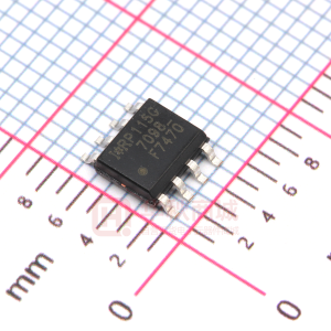
IRF7470
HEXFET® Power MOSFET
VDSS
40V
RDS(on) max
13mΩ
ID
10A
Benefits
l l l
Ultra-Low Gate Impedance Very Low RDS(on) at 4.5V VGS Fully Characterized Avalanche Voltage and Current
S S S G
1 8 7
A A D D D D
2
3
6
4
5
T o p V ie w
SO-8
Absolute Maximum Ratings
Symbol
VDS VGS ID @ TA = 25°C ID @ TA = 70°C IDM PD @TA = 25°C PD @TA = 70°C TJ , TSTG
Parameter
Drain-Source Voltage Gate-to-Source Voltage Continuous Drain Current, VGS @ 10V Continuous Drain Current, VGS @ 10V Pulsed Drain Current Maximum Power Dissipation Maximum Power Dissipation Linear Derating Factor Junction and Storage Temperature Range
Max.
40 ± 12 10 8.5 85 2.5 1.6 0.02 -55 to + 150
Units
V V A W W mW/°C °C
Thermal Resistance
Symbol
RθJL RθJA
Parameter
Junction-to-Drain Lead Junction-to-Ambient
Typ.
––– –––
Max.
20 50
Units
°C/W
Notes through are on page 8
www.irf.com
1
3/25/01
�IRF7470
Static @ TJ = 25°C (unless otherwise specified)
Parameter Drain-to-Source Breakdown Voltage ∆V(BR)DSS/∆TJ Breakdown Voltage Temp. Coefficient V(BR)DSS RDS(on) VGS(th) IDSS IGSS Min. 40 ––– ––– Static Drain-to-Source On-Resistance ––– ––– Gate Threshold Voltage 0.8 ––– Drain-to-Source Leakage Current ––– Gate-to-Source Forward Leakage ––– Gate-to-Source Reverse Leakage ––– Typ. Max. Units ––– ––– V 0.04 ––– V/°C 9.0 13 10 15 mΩ 14.5 30 ––– 2.0 V ––– 20 µA ––– 100 ––– 200 nA ––– -200 Conditions VGS = 0V, ID = 250µA Reference to 25°C, ID = 1mA VGS = 10V, ID = 10A VGS = 4.5V, ID = 8.0A VGS = 2.8V, ID = 5.0A VDS = VGS, ID = 250µA VDS = 32V, VGS = 0V VDS = 32V, VGS = 0V, T J = 125C VGS = 12V VGS = -12V
Dynamic @ TJ = 25°C (unless otherwise specified)
Symbol
gfs Qg Qgs Qgd Qoss td(on) tr td(off) tf Ciss Coss Crss Parameter Forward Transconductance Total Gate Charge Gate-to-Source Charge Gate-to-Drain ("Miller") Charge Output Gate Charge Turn-On Delay Time Rise Time Turn-Off Delay Time Fall Time Input Capacitance Output Capacitance Reverse Transfer Capacitance Min. 27 ––– ––– ––– ––– ––– ––– ––– ––– ––– ––– ––– Typ. ––– 29 7.9 8.0 23 10 1.9 21 3.2 3430 690 41 Max. Units Conditions ––– S VDS = 20V, ID = 8.0A 44 ID = 8.0A 12 nC VDS = 20V 12 VGS = 4.5V 35 VGS = 0V, VDS = 16V ––– VDD = 20V ––– ID = 8.0A ns ––– RG = 1.8Ω ––– VGS = 4.5V ––– VGS = 0V ––– VDS = 20V ––– pF ƒ = 1.0MHz
Avalanche Characteristics
Symbol
EAS IAR
Parameter
Single Pulse Avalanche Energy Avalanche Current
Typ.
––– –––
Max.
300 8.0
Units
mJ A
Diode Characteristics
Symbol
IS
ISM
Parameter Continuous Source Current (Body Diode) Pulsed Source Current (Body Diode) Diode Forward Voltage Reverse Reverse Reverse Reverse Recovery Recovery Recovery Recovery Time Charge Time Charge
Min. Typ. Max. Units ––– ––– ––– ––– 2.3 A 85 1.3 ––– 110 200 110 230 V ns nC ns nC
VSD trr Qrr trr Qrr
––– 0.80 ––– 0.65 ––– 72 ––– 130 ––– 76 ––– 150
Conditions D MOSFET symbol showing the G integral reverse S p-n junction diode. TJ = 25°C, IS = 8.0A, VGS = 0V TJ = 125°C, IS = 8.0A, VGS = 0V TJ = 25°C, IF = 8.0A, VR= 20V di/dt = 100A/µs TJ = 125°C, IF = 8.0A, VR=20V di/dt = 100A/µs
2
www.irf.com
�IRF7470
1000
VGS 15V 10V 4.5V 3.0V 2.7V 2.5V 2.25V BOTTOM 2.0V TOP
100
I D , Drain-to-Source Current (A)
100
I D , Drain-to-Source Current (A)
VGS 15V 10V 4.5V 3.0V 2.7V 2.5V 2.25V BOTTOM 2.0V TOP
2.0V
10
10
2.0V
20µs PULSE WIDTH TJ = 25 °C
1 10 100
1 0.1
1 0.1
20µs PULSE WIDTH TJ = 150 °C
1 10 100
VDS , Drain-to-Source Voltage (V)
VDS , Drain-to-Source Voltage (V)
Fig 1. Typical Output Characteristics
Fig 2. Typical Output Characteristics
100
2.5
TJ = 150 ° C
R DS(on) , Drain-to-Source On Resistance (Normalized)
ID = 10A
I D , Drain-to-Source Current (A)
2.0
TJ = 25 ° C
10
1.5
1.0
0.5
1 2.0
V DS = 25V 20µs PULSE WIDTH 2.2 2.4 2.6 2.8 3.0
0.0 -60 -40 -20
VGS = 10V
0 20 40 60 80 100 120 140 160
VGS , Gate-to-Source Voltage (V)
TJ , Junction Temperature ( °C)
Fig 3. Typical Transfer Characteristics
Fig 4. Normalized On-Resistance Vs. Temperature
www.irf.com
3
�IRF7470
100000 10 VGS = 0V, f = 1 MHZ Ciss = C + Cgd, C gs ds SHORTED Crss = C gd Coss = C + Cgd ds
ID = 8.0A VDS = 32V VDS = 20V
VGS , Gate-to-Source Voltage (V)
8
10000
C, Capacitance(pF)
Ciss
1000
6
Coss
4
100
2
Crss
10 1 10 100
0 0 10 20 30 40 50 60
VDS, Drain-to-Source Voltage (V)
QG , Total Gate Charge (nC)
Fig 5. Typical Capacitance Vs. Drain-to-Source Voltage
Fig 6. Typical Gate Charge Vs. Gate-to-Source Voltage
100
1000
OPERATION IN THIS AREA LIMITED BY RDS(on)
ISD , Reverse Drain Current (A)
TJ = 150 ° C
10
I D , Drain Current (A)
100 10us
TJ = 25 ° C
1
100us 10 1ms
0.1 0.2
V GS = 0 V
0.6 1.0 1.4 1.8 2.2
1 0.1
TA = 25 ° C TJ = 150 ° C Single Pulse
1 10
10ms
100
VSD ,Source-to-Drain Voltage (V)
VDS , Drain-to-Source Voltage (V)
Fig 7. Typical Source-Drain Diode Forward Voltage
Fig 8. Maximum Safe Operating Area
4
www.irf.com
�Fig 6. On-Resistance Vs. Drain Current
IRF7470
10.0
VDS
8.0
RD
VGS RG
D.U.T.
+
I D , Drain Current (A)
-VDD
6.0
10V
4.0
Pulse Width ≤ 1 µs Duty Factor ≤ 0.1 %
Fig 10a. Switching Time Test Circuit
2.0
VDS 90%
0.0 25 50 75 100 125 150
TC , Case Temperature
( °C)
10% VGS
td(on) tr t d(off) tf
Fig 10b. Switching Time Waveforms
100
Thermal Response (Z thJA )
D = 0.50 10 0.20 0.10 0.05 1 0.02 0.01 P DM t1 0.1 SINGLE PULSE (THERMAL RESPONSE) Notes: 1. Duty factor D = t 1 / t 2 2. Peak T J = P DM x Z thJA + TA 0.0001 0.001 0.01 0.1 1 10 100 t2
0.01 0.00001
t1 , Rectangular Pulse Duration (sec)
Fig 10. Maximum Effective Transient Thermal Impedance, Junction-to-Ambient
www.irf.com
5
�IRF7470
R DS (on) , Drain-to-Source On Resistance ( Ω )
R DS(on) , Drain-to -Source On Resistance ( Ω )
0.030
0.020
0.018
0.025
0.016
0.020
0.014
VGS = 2.7V 0.015 VGS = 4.5V 0.010 0 10 20 30 VGS = 10V 40 50 60
ID = 10A
0.012
0.010 2 4 6 8 10 12 14 16
ID , Drain Current (A)
VGS, Gate -to -Source Voltage (V)
Fig 12. On-Resistance Vs. Drain Current
Current Regulator Same Type as D.U.T.
Fig 13. On-Resistance Vs. Gate Voltage
50KΩ 12V .2µF .3µF
VGS
QGS
D.U.T. + V - DS
QG QGD
800
EAS , Single Pulse Avalanche Energy (mJ)
VG
VGS
3mA
TOP BOTTOM
600
Charge
IG ID
ID 3.6A 6.4A 8.0A
Current Sampling Resistors
Fig 13a&b. Basic Gate Charge Test Circuit and Waveform
400
15 V
200
V (B R )D S S tp VD S L DRIVE R
RG 20V IAS tp
D .U .T IA S 0.01 Ω
+ V - DD
0 25 50 75 100 125 150
A
Starting TJ , Junction Temperature ( °C)
Fig 14a&b. Unclamped Inductive Test circuit and Waveforms
Fig 14c. Maximum Avalanche Energy Vs. Drain Current
6
www.irf.com
�IRF7470
SO-8 Package Details
D -B-
D IM
5
IN C H E S M IN .05 32 .00 40 .01 4 .00 75 .18 9 .15 0 M AX .06 88 .00 98 .01 8 .009 8 .196 .15 7
M ILLIM E T E R S M IN 1.3 5 0.1 0 0.3 6 0.19 4.80 3.8 1 M AX 1.75 0.25 0.46 0.25 4.98 3.99
A
6 5 H 0 .2 5 (.0 1 0 ) M AM
5
8 E -A-
7
A1 B C D E e e1 H K
0 .1 0 (.0 0 4 ) L 8X 6 C 8X
1
2
3
4
e 6X
e1 A
θ
θ
K x 4 5°
.05 0 B A S IC .02 5 B A S IC .22 84 .01 1 0.16 0° .244 0 .01 9 .05 0 8°
1.27 B A S IC 0 .635 B A S IC 5.8 0 0.2 8 0.4 1 0° 6.20 0.48 1.27 8°
-C B 8X 0 .2 5 (.0 1 0 ) A1 M CASBS
L θ
R E C O M M E N D E D F O O T P R IN T 0 .7 2 (.0 2 8 ) 8X
NOTES: 1 . D IM E N S IO N IN G A N D T O L E R A N C IN G P E R A N S I Y 1 4 .5 M -1 9 8 2 . 2 . C O N T R O L L IN G D IM E N S IO N : IN C H . 3 . D IM E N S IO N S A R E S H O W N IN M IL L IM E T E R S (IN C H E S ). 4 . O U T L IN E C O N F O R M S T O J E D E C O U T L IN E M S -0 1 2 A A . 5 D IM E N S IO N D O E S N O T IN C L U D E M O L D P R O T R U S IO N S M O L D P R O T R U S IO N S N O T T O E X C E E D 0 .2 5 (.0 0 6 ). 6 D IM E N S IO N S IS T H E L E N G T H O F L E A D F O R S O L D E R IN G T O A S U B S T R A T E ..
6 .4 6 ( .2 5 5 )
1 .7 8 (.0 7 0 ) 8X
1 .2 7 ( .0 5 0 ) 3X
SO-8 Part Marking
www.irf.com
7
�IRF7470
SO-8 Tape and Reel
TER M IN AL N UM B ER 1
1 2.3 ( .484 ) 1 1.7 ( .461 )
8.1 ( .318 ) 7.9 ( .312 )
F EE D D IRE C TIO N
N OT E S : 1 . CO NT RO L L ING DIM E NSIO N : M IL L IM E T E R . 2 . AL L DIM E NS ION S ARE SHO W N IN M ILL IM E TER S ( INC HE S ) . 3 . OU TL IN E CO N FO RM S T O E IA -4 8 1 & E IA -5 4 1 .
3 3 0.00 (12.992) M AX .
14.4 0 ( .566 ) 12.4 0 ( .488 ) N O T ES : 1 . CO NT RO LL ING D IM EN SIO N : M ILLIME TER . 2 . O U TLIN E C O NF O RM S T O E IA-48 1 & E IA -54 1.
Notes:
Repetitive rating; pulse width limited by
max. junction temperature.
Pulse width ≤ 400µs; duty cycle ≤ 2%. When mounted on 1 inch square copper board, t