PD- 95143
SMPS MOSFET
Applications Switch Mode Power Supply (SMPS) l Uninterruptible Power Supply l High Speed Power Switching l Lead-Free
l
HEXFET® Power MOSFET
IRF840ASPbF IRF840ALPbF ID
8.0A
VDSS
500V
RDS(on) max
0.85Ω
Benefits l Low Gate Charge Qg Results in Simple Drive Requirement l Improved Gate, Avalanche and Dynamic dv/dt Ruggedness l Fully Characterized Capacitance and Avalanche Voltage and Current l Effective Coss Specified (See AN 1001)
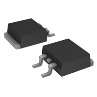
D2Pak IRF840AS
TO-262 IRF840AL
Absolute Maximum Ratings
Parameter
ID @ TC = 25°C ID @ TC = 100°C IDM PD @TC = 25°C PD @TA = 25°C VGS dv/dt TJ TSTG Continuous Drain Current, VGS @ 10V Continuous Drain Current, VGS @ 10V Pulsed Drain Current Power Dissipation Power Dissipation Linear Derating Factor Gate-to-Source Voltage Peak Diode Recovery dv/dt Operating Junction and Storage Temperature Range Soldering Temperature, for 10 seconds
Max.
8.0 5.1 32 125 3.1 1.0 ± 30 5.0 -55 to + 150 300 (1.6mm from case )
Units
A W W/°C V V/ns °C
Typical SMPS Topologies
l l l
Two Transistor Forward Haft Bridge Full Bridge
through are on page 10
Notes
www.irf.com
1
04/21/04
�IRF840AS/LPbF
Static @ TJ = 25°C (unless otherwise specified)
V(BR)DSS
∆V(BR)DSS/∆TJ
RDS(on) VGS(th) IDSS IGSS
Parameter Drain-to-Source Breakdown Voltage Breakdown Voltage Temp. Coefficient Static Drain-to-Source On-Resistance Gate Threshold Voltage Drain-to-Source Leakage Current Gate-to-Source Forward Leakage Gate-to-Source Reverse Leakage Parameter Forward Transconductance Total Gate Charge Gate-to-Source Charge Gate-to-Drain ("Miller") Charge Turn-On Delay Time Rise Time Turn-Off Delay Time Fall Time Input Capacitance Output Capacitance Reverse Transfer Capacitance Output Capacitance Output Capacitance Effective Output Capacitance
Min. 500 ––– ––– 2.0 ––– ––– ––– ––– Min. 3.7 ––– ––– ––– ––– ––– ––– ––– ––– ––– ––– ––– ––– –––
Typ. ––– 0.58 ––– ––– ––– ––– ––– ––– Typ. ––– ––– ––– ––– 11 23 26 19 1018 155 8.0 1490 42 56
Max. Units Conditions ––– V VGS = 0V, ID = 250µA ––– V/°C Reference to 25°C, ID = 1mA 0.85 Ω VGS = 10V, ID = 4.8A 4.0 V VDS = VGS, ID = 250µA 25 VDS = 500V, VGS = 0V µA 250 VDS = 400V, VGS = 0V, TJ = 125°C 100 VGS = 30V nA -100 VGS = -30V Max. Units Conditions ––– S VDS = 50V, ID = 4.8A 38 ID = 8.0A 9.0 nC VDS = 400V 18 VGS = 10V, See Fig. 6 and 13 ––– VDD = 250V ––– ID = 8.0A ns ––– RG = 9.1Ω ––– RD = 31Ω,See Fig. 10 ––– VGS = 0V ––– VDS = 25V ––– pF ƒ = 1.0MHz, See Fig. 5 ––– VGS = 0V, VDS = 1.0V, ƒ = 1.0MHz ––– VGS = 0V, VDS = 400V, ƒ = 1.0MHz ––– VGS = 0V, VDS = 0V to 480V
Dynamic @ TJ = 25°C (unless otherwise specified)
gfs Qg Qgs Qgd td(on) tr td(off) tf Ciss Coss Crss Coss Coss Coss eff.
Avalanche Characteristics
Parameter
EAS IAR EAR Single Pulse Avalanche Energy Avalanche Current Repetitive Avalanche Energy
Typ.
––– ––– –––
Max.
510 8.0 13
Units
mJ A mJ
Thermal Resistance
Parameter
RθJC RθJA Junction-to-Case Junction-to-Ambient ( PCB Mounted, steady-state)* Parameter Continuous Source Current (Body Diode) Pulsed Source Current (Body Diode) Diode Forward Voltage Reverse Recovery Time Reverse RecoveryCharge Forward Turn-On Time
Typ.
––– –––
Max.
1.0 40
Units
°C/W
Diode Characteristics
Min. Typ. Max. Units IS
ISM
VSD trr Qrr ton
Conditions D MOSFET symbol ––– ––– 8.0 showing the A G integral reverse ––– ––– 32 S p-n junction diode. ––– ––– 2.0 V TJ = 25°C, IS = 8.0A, VGS = 0V ––– 422 633 ns TJ = 25°C, IF = 8.0A ––– 2.0 3.0 µC di/dt = 100A/µs Intrinsic turn-on time is negligible (turn-on is dominated by LS+LD)
2
www.irf.com
�IRF840AS/LPbF
100
I D , Drain-to-Source Current (A)
I D , Drain-to-Source Current (A)
10
�
VGS 15V 10V 8.0V 7.0V 6.0V 5.5V 5.0V BOTTOM 4.5V TOP
100
10
�
VGS 15V 10V 8.0V 7.0V 6.0V 5.5V 5.0V BOTTOM 4.5V TOP
4.5V
1
1
4.5V
20µs PULSE WIDTH � T = 25 C
J ° 1 10 100
0.1 0.1
VDS , Drain-to-Source Voltage (V)
0.1 0.1
20µs PULSE WIDTH � T = 150 C
J ° 1 10 100
VDS , Drain-to-Source Voltage (V)
Fig 1. Typical Output Characteristics
Fig 2. Typical Output Characteristics
100
3.0
ID 8.0 � = 7.4A
R DS(on) , Drain-to-Source On Resistance (Normalized)
I D , Drain-to-Source Current (A)
2.5
10
TJ = 150 ° C �
2.0
TJ = 25 ° C �
1
1.5
1.0
0.5
0.1 4.0
�
V DS = 50V 20µs PULSE WIDTH 7.0 8.0 5.0 6.0 9.0
0.0 -60 -40 -20
VGS = 10V �
0 20 40 60 80 100 120 140 160
VGS , Gate-to-Source Voltage (V)
TJ , Junction Temperature ( °C)
Fig 3. Typical Transfer Characteristics
Fig 4. Normalized On-Resistance Vs. Temperature
www.irf.com
3
�IRF840AS/LPbF
100000 VGS = 0V, f = 1 MHZ Ciss = C + C , C gs gd ds SHORTED Crss = C gd Coss = C + C ds gd
20
8.0 ID = 7.4 A �
VGS , Gate-to-Source Voltage (V)
10000
16
�
VDS = 400V VDS = 250V VDS = 100V
C, Capacitance(pF)
1000
Ciss Coss
12
100
8
10
Crss
4
1 1 10 100 1000
0
�
FOR TEST CIRCUIT SEE FIGURE 13
30 0 10 20 40
VDS, Drain-to-Source Voltage (V)
Q G , Total Gate Charge (nC)
Fig 5. Typical Capacitance Vs. Drain-to-Source Voltage
Fig 6. Typical Gate Charge Vs. Gate-to-Source Voltage
100
100
ISD , Reverse Drain Current (A)
OPERATION IN THIS AREA LIMITED BY R �
DS(on)
� 10us
10
I D , Drain Current (A)
TJ = 150 ° C �
10
� 100us
� 1ms
1
1
TJ = 25 ° C �
� 10ms
0.1 0.2
V GS = 0 V �
0.5 0.8 1.1 1.4
0.1
�
TC = 25 °C TJ = 150 °C Single Pulse
10 100 1000 10000
VSD ,Source-to-Drain Voltage (V)
VDS , Drain-to-Source Voltage (V)
Fig 7. Typical Source-Drain Diode Forward Voltage
Fig 8. Maximum Safe Operating Area
4
www.irf.com
�IRF840AS/LPbF
8.0
VDS VGS
RD
I D , Drain Current (A)
6.0
RG
D.U.T.
+
-VDD
10V
4.0
Pulse Width ≤ 1 µs Duty Factor ≤ 0.1 %
2.0
Fig 10a. Switching Time Test Circuit
VDS 90%
0.0
25
50
75
100
125
150
TC , Case Temperature
( °C)
10% VGS
td(on) tr t d(off) tf
Fig 9. Maximum Drain Current Vs. Case Temperature
Fig 10b. Switching Time Waveforms
10
Thermal Response (Z thJC )
1 D = 0.50 0.20 0.1 0.10 0.05 0.02 0.01
�
SINGLE PULSE (THERMAL RESPONSE) 0.0001 0.001 0.01
0.01 0.00001
�
Notes: 1. Duty factor D = t 1 / t 2 2. Peak T J = P DM x Z thJC + TC 0.1
�
P DM t1 t2 1
t1 , Rectangular Pulse Duration (sec)
www.irf.com
5
�IRF840AS/LPbF
1 5V
1200
EAS , Single Pulse Avalanche Energy (mJ)
VDS
L
D R IV E R
1000
�
TOP BOTTOM ID 3.6A 5.1A 8.0A
800
RG
20V
D .U .T
IA S tp
+ V - DD
A
600
0 .0 1 Ω
Fig 12a. Unclamped Inductive Test Circuit
V (B R )D SS tp
400
200
0
25
50
75
100
125
150
Starting TJ , Junction Temperature ( °C)
IAS
Fig 12b. Unclamped Inductive Waveforms
QG
Fig 12c. Maximum Avalanche Energy Vs. Drain Current
10 V
QGS
QGD
610
VG
V DSav , Avalanche Voltage ( V )
600 590 580 570 560 550 540
Charge
Fig 13a. Basic Gate Charge Waveform
Current Regulator Same Type as D.U.T.
50KΩ 12V .2µF .3µF
D.U.T. VGS
3mA
+ V - DS
0.0
1.0
2.0
3.0
4.0
5.0
6.0
IAV , Avalanche Current ( A)
IG ID
Current Sampling Resistors
Fig 13b. Gate Charge Test Circuit
Fig 12d. Typical Drain-to-Source Voltage Vs. Avalanche Current
6
www.irf.com
�IRF840AS/LPbF
Peak Diode Recovery dv/dt Test Circuit
D.U.T
+
+
Circuit Layout Considerations • Low Stray Inductance • Ground Plane • Low Leakage Inductance Current Transformer
-
+
RG • • • • dv/dt controlled by RG Driver same type as D.U.T. ISD controlled by Duty Factor "D" D.U.T. - Device Under Test
+ VDD
Driver Gate Drive P.W. Period D=
P.W. Period VGS=10V
*
D.U.T. ISD Waveform Reverse Recovery Current Body Diode Forward Current di/dt D.U.T. VDS Waveform Diode Recovery dv/dt
VDD
Re-Applied Voltage Inductor Curent
Body Diode
Forward Drop
Ripple ≤ 5%
ISD
* VGS = 5V for Logic Level Devices Fig 14. For N-Channel HEXFET® Power MOSFETs
www.irf.com
7
�IRF840AS/LPbF
D2Pak Package Outline
Dimensions are shown in millimeters (inches)
D2Pak Part Marking Information (Lead-Free)
T H IS IS AN IR F 5 30 S WIT H L OT CODE 80 24 AS S E MB L E D ON WW 0 2, 2 000 IN T H E AS S E MB L Y L IN E "L " N ote: "P " in as s embly line pos ition indicates "L ead-F ree" IN T E R N AT ION AL R E CT IF IE R L OGO AS S E MB L Y L OT CODE P AR T NU MB E R F 53 0S D AT E CODE YE AR 0 = 20 00 WE E K 02 L IN E L
OR
INT E R N AT ION AL R E CT IF IE R L OGO AS S E MB L Y L OT CODE P AR T NU MB E R F 530S DAT E CODE P = DE S IGNAT E S L E AD-F R E E P R ODU CT (OP T IONAL ) YE AR 0 = 20 00 WE E K 02 A = AS S E MB L Y S IT E CODE
8
www.irf.com
�IRF840AS/LPbF
TO-262 Package Outline
Dimensions are shown in millimeters (inches)
TO-262 Part Marking Information
E XAMP L E : T H IS IS AN IR L 3103L L OT CODE 1789 AS S E MB L E D ON WW 19, 1997 IN T H E AS S E MB L Y L INE "C" Note: "P " in as s embly line pos ition indicates "L ead-F ree" IN T E R NAT IONAL R E CT IF IE R L OGO AS S E MB L Y L OT CODE P AR T NU MB E R
DAT E CODE YE AR 7 = 1997 WE E K 19 L INE C
OR
IN T E R NAT IONAL R E CT IF IE R L OGO AS S E MB L Y L OT CODE P AR T NU MB E R DAT E CODE P = DE S IGNAT E S L E AD-F R E E P R ODU CT (OP T IONAL ) YE AR 7 = 1997 WE E K 19 A = AS S E MB L Y S IT E CODE
www.irf.com
9
�IRF840AS/LPbF
D2Pak Tape & Reel InforTRR
1 .6 0 ( .06 3 ) 1 .5 0 ( .05 9 ) 4 .10 ( .1 6 1 ) 3 .90 ( .1 5 3 )
1 .6 0 ( .0 6 3 ) 1 .5 0 ( .0 5 9 )
0 .3 6 8 ( .0 1 4 5 ) 0 .3 4 2 ( .0 1 3 5 )
F E E D D IR E C T I O N
1 .8 5 ( .07 3 ) 1 .6 5 ( .06 5 )
1 1 .6 0 ( .4 5 7 ) 1 1 .4 0 ( .4 4 9 )
1 5 .4 2 ( .6 0 9 ) 1 5 .2 2 ( .6 0 1 )
2 4 .3 0 ( .9 5 7 ) 2 3 .9 0 ( .9 4 1 )
TRL
1 0 . 9 0 ( .4 2 9 ) 1 0 . 7 0 ( .4 2 1 ) 1 .7 5 ( .0 6 9 ) 1 .2 5 ( .0 4 9 ) 1 6 .1 0 ( .6 3 4 ) 1 5 .9 0 ( .6 2 6 ) 4 .7 2 ( .1 3 6 ) 4 .5 2 ( .1 7 8 )
F E E D D I R E C T IO N
1 3 .5 0 ( .5 3 2 ) 1 2 .8 0 ( .5 0 4 )
2 7 .40 ( 1 .0 79 ) 2 3 .90 ( .9 4 1 ) 4
330.00 ( 14.173 ) M A X.
6 0 .00 ( 2 .3 6 2 ) M IN .
N OT ES : 1 . C O M F O R M S T O E IA -4 1 8. 2 . C O N T R O LL IN G D IM E N S IO N : M IL L IM E T E R . 3 . D IM E N S IO N M E A S U R E D @ H U B . 4 . IN C L U D E S F LA N G E D IS T O R T IO N @ O U T E R E D G E .
3 0.4 0 ( 1 .1 97 ) M AX. 26.40 ( 1.039 ) 24.40 ( .961 )
4
3
Notes:
Repetitive rating; pulse width limited by Starting TJ = 25°C, L = 16mH
TJ ≤ 150°C RG = 25Ω, IAS = 8.0A. (See Figure 12)
max. junction temperature. (See fig. 11)
Pulse width ≤ 300µs; duty cycle ≤ 2%.
Coss eff. is a fixed capacitance that gives the same charging time
as Coss while VDS is rising from 0 to 80% VDSS
ISD ≤ 8.0A, di/dt ≤ 100A/µs, VDD ≤ V(BR)DSS,
Uses IRF840A data and test conditions
* When mounted on 1" square PCB ( FR-4 or G-10 Material ). For recommended footprint and soldering techniques refer to application note #AN-994.
Data and specifications subject to change without notice.
IR WORLD HEADQUARTERS: 233 Kansas St., El Segundo, California 90245, USA Tel: (310) 252-7105 TAC Fax: (310) 252-7903 Visit us at www.irf.com for sales contact information. 04/04
10
www.irf.com
�