PD- 96095
IRF9Z30PbF
Features
P-Channel Verasatility Compact Plastic Package Fast Switching Low Drive Current Ease of Paralleling Excellent Temperature Stability L ead-Free
HEXFET® POWER MOSFET
Product Summary
Part Number IRF9Z30PbF VDS(V) -50
D
RDSON (Ω) 0.14
ID (A) -18
G
Description
S
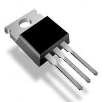
TO-220AB
The HEXFET® technology is the key to International Rectifier’s advanced line of power MOSFET transistors. The efficient geometry and unique processing of the HEXFET design achieve very low on-state resistence combined with high transconductance and extreme device ruggedness. The P-Channel HEXFETs are designed for applications which require the convenience of reverse polarity operation. They retain all of the features of the more common N-Channel HEXFETs such as voltage control, very fast switching, ease of paralleling, and excellent temperature stability. P-Channel HEXFETs are intended for use in power stages where complementary symmetry with N-Channel devices offers circuit simplification. They are also very useful in drive stages because of the circuit versatility offered by the reverse polarity connection. Applications include motor control, audio amplifiers, switched mode converters, control circuit and pulse amplifiers.
Absolute Maximum Ratings
Parameter
VDS VDGR VGS ID @ TC = 25°C ID @ TC = 100°C IDM PD @TC = 25°C ILM IL TJ TSTG Lead Temperature Drain-to-Source Voltage Drain-to-Gate Voltage (RGS =20KΩ) Gate-to-Source Voltage Continuous Drain Current, VGS Continuous Drain Current, VGS Pulsed Drain Current Max. Power Dissipation Linear Derating Factor Inductive Current, Clamped (L= 100µH) See Fig. 14 Unclamped Inductive Current(Avalanche Current) Operating Junction and Storage Temperature Range 300 (0.063 in. (1.6mm) from case for 10s) See Fig. 15
Max.
-50 -50 ±20 -18 -11 -60 74 0.59 -60 -3.1 -55 to + 150
Units
V
A W W/°C A
°C
Thermal Resistance
Parameter
RθJC RθCS RθJA J unction-to-Case Case-to-Sink, Flat, Greased Surface J unction-to-Ambient
Typ.
––– 1.0 –––
Max.
1.7 ––– 80
Units
°C/W
www.irf.com
03/27/07
1
�IRF9Z30PbF
Electrical Characteristics @ TJ = 25°C (unless otherwise specified) Parameter
BVDSS VGS(th) IGSS IDSS ID(on) gfs Ciss Coss Crss td(on) tr td(off) tf Qg Qgs Qgd LD Drain-to-Source Breakdown Voltage Gate Threshold Voltage Gate-to-Source Forward Leakage Gate-to-Source Reverse Leakage Drain-to-Source Leakage Current On- State Drain Current Forward Transconductance Input Capacitance Output Capacitance Reverse Transfer Capacitance Turn-On Delay Time Rise Time Turn-Off Delay Time Fall Time Total Gate Charge (Gate -Source Plus Gate-Drain) Post-Vth Gate-to-Source Charge Gate-to-Drain Charge Internal Drain Inductance ––– LS Internal Source Inductance ––– 7.5 ––– 4.5 ––– nH
Min. Typ. Max. Units
-50 -2.0 ––– ––– ––– ––– -18 ––– 3.1 ––– ––– ––– ––– ––– ––– ––– ––– ––– ––– ––– ––– ––– ––– ––– ––– ––– 4.7 900 570 140 12 110 21 64 26 6.9 9.7 ––– -4.0 -500 500 -250 -1000 ––– ––– ––– ––– ––– 18 170 32 96 39 10 15 ns pF V V nA µA A Ω S
Conditions
VGS = 0V, ID = -250µA VDS = VGS, ID = -250µA VGS = -20V VGS = 20V VDS = Max. Rating, VGS = 0V VDS = Max. Rating x 0.8, VGS = 0V, TJ = 125°C VDS > ID(on) X RDS(ON) (max)., VGS = -10V VGS = -10V, ID = -9.3A VDS = 2 X VGS, IDS = -9.0A VGS = 0V VDS = -25V ƒ = 1.0MHz, See Fig.16 (MOSFET switching times are assentially independent of operating temperature) VGS = -10V, ID = -18A, VDS = 0.8 Max. Rating See Fig.10 VDD = -25V, ID = -18A, RG = 13Ω, RD = 1.3Ω
RDS(on) Static Drain-to-Source On-Resistance
0.093 0.14
nC See Fig.17 for test circuit (Gate charge is essentially independent of operating temperature.)
Measured from the drain lead, 6mm (0.25 in.) from package to center of die. Measured from the source lead, 6mm (0.25 in.) from package to source bonding pad.
Modified MOSFET symbol showing the internal device inductances.
Source-Drain Diode Ratings and Characteristics IS ISM VSD trr Qrr Ton Parameter Continuous Source Current (Body Diode) Pulsed Source Current (Body Diode) Diode Forward Voltage Reverse Recovery Time Reverse Recovery Charge Forward Turn-on Time Min. Typ. Max. Units ––– ––– ––– 54 ––– ––– ––– 120 -18 A -60 -6.3 250 1.1 V MOSFET symbol showing the integral reverse p-n junction rectifier. TJ = 25°C, IS = -18A, VGS = 0V Conditions
0.20 0.47
ns TJ = 25°C, IF = -18A µC di/dt = 100A/µs
Intrinsic turn-on time is negligible. Turn-on speed is substantially controlled by LS + LD.
Note:
TJ = 25°C to 150°C Repetitive Rating :Pulse width limited by max. junction tempeature. See Transient Thermal Impedance Curve (Fig.5). @ Vdd = -25V, TJ= 25°C, L = 100µH, R G = 25Ω. Pulse Test : Pulse width ≤ 300ms, Duty Cycle ≤ 2%.
2
www.irf.com
�IRF9Z30PbF
www.irf.com
3
�IRF9Z30PbF
4
www.irf.com
�IRF9Z30PbF
www.irf.com
5
�IRF9Z30PbF
6
www.irf.com
�IRF9Z30PbF
TO-220AB Package Outline
Dimensions are shown in millimeters (inches)
TO-220AB Part Marking Information
EXAMPLE: THIS IS AN IRF1010 LOT CODE 1789 ASSEMBLED ON WW 19, 2000 IN THE ASSEMBLY LINE "C" Note: "P" in assembly line position indicates "Lead - Free" INTERNATIONAL RECTIFIER LOGO ASSEMBLY LOT CODE PART NUMBER
DATE CODE YEAR 0 = 2000 WEEK 19 LINE C
Data and specifications subject to change without notice. This product has been designed and qualified for the Industrial market. Qualification Standards can be found on IR’s Web site.
IR WORLD HEADQUARTERS: 233 Kansas St., El Segundo, California 90245, USA Tel: (310) 252-7105 TAC Fax: (310) 252-7903 Visit us at www.irf.com for sales contact information. 03/2007
www.irf.com
7
�
很抱歉,暂时无法提供与“IRF9Z30PBF”相匹配的价格&库存,您可以联系我们找货
免费人工找货