PD - 96901A
IRFB3307 IRFS3307 IRFSL3307
Applications l High Efficiency Synchronous Rectification in SMPS l Uninterruptible Power Supply l High Speed Power Switching l Hard Switched and High Frequency Circuits Benefits l Improved Gate, Avalanche and Dynamic dV/dt Ruggedness l Fully Characterized Capacitance and Avalanche SOA l Enhanced body diode dV/dt and dI/dt Capability
G S
HEXFET® Power MOSFET
D
VDSS RDS(on) typ. max. ID
75V 5.0m: 6.3m: 130A
GDS
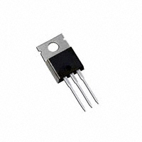
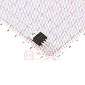
TO-220AB IRFB3307
GDS
D2Pak IRFS3307
GDS
TO-262 IRFSL3307
Absolute Maximum Ratings
Symbol
ID @ TC = 25°C ID @ TC = 100°C IDM PD @TC = 25°C VGS dv/dt TJ TSTG
Parameter
Continuous Drain Current, VGS @ 10V Continuous Drain Current, VGS @ 10V Pulsed Drain Current d Maximum Power Dissipation Linear Derating Factor Gate-to-Source Voltage Peak Diode Recovery f Operating Junction and Storage Temperature Range Soldering Temperature, for 10 seconds (1.6mm from case) Mounting torque, 6-32 or M3 screw Single Pulse Avalanche Energy e Avalanche Current c Repetitive Avalanche Energy g
Max.
130c 91c 510 250 1.6 ± 20 11 -55 to + 175 300 10lbxin (1.1Nxm) 270 See Fig. 14, 15, 16a, 16b
Units
A
W W/°C V V/ns °C
Avalanche Characteristics
EAS (Thermally limited) IAR EAR mJ A mJ
Thermal Resistance
Symbol
RθJC RθCS RθJA RθJA
Parameter
Junction-to-Case k Case-to-Sink, Flat Greased Surface , TO-220 Junction-to-Ambient, TO-220 k Junction-to-Ambient (PCB Mount) , D Pak jk
2
Typ.
––– 0.50 ––– –––
Max.
0.61 ––– 62 40
Units
°C/W
www.irf.com
1
11/04/04
�IRFB3307/IRFS3307/IRFSL3307
Static @ TJ = 25°C (unless otherwise specified)
Symbol
V(BR)DSS ∆V(BR)DSS/∆TJ RDS(on) VGS(th) IDSS IGSS RG
Parameter
Drain-to-Source Breakdown Voltage Breakdown Voltage Temp. Coefficient Static Drain-to-Source On-Resistance Gate Threshold Voltage Drain-to-Source Leakage Current Gate-to-Source Forward Leakage Gate-to-Source Reverse Leakage Gate Input Resistance
Min. Typ. Max. Units
75 ––– ––– 2.0 ––– ––– ––– ––– ––– ––– ––– 0.069 ––– 5.0 6.3 ––– 4.0 ––– 20 ––– 250 ––– 200 ––– -200 1.5 –––
Conditions
V VGS = 0V, ID = 250µA V/°C Reference to 25°C, ID = 1mAd mΩ VGS = 10V, ID = 75A g V VDS = VGS, ID = 150µA µA VDS = 75V, VGS = 0V VDS = 75V, VGS = 0V, TJ = 125°C nA VGS = 20V VGS = -20V Ω f = 1MHz, open drain
Dynamic @ TJ = 25°C (unless otherwise specified)
Symbol
gfs Qg Qgs Qgd td(on) tr td(off) tf Ciss Coss Crss Coss eff. (ER) Coss eff. (TR)
Parameter
Forward Transconductance Total Gate Charge Gate-to-Source Charge Gate-to-Drain ("Miller") Charge Turn-On Delay Time Rise Time Turn-Off Delay Time Fall Time Input Capacitance Output Capacitance Reverse Transfer Capacitance
Min. Typ. Max. Units
––– 120 35 46 26 120 51 63 5150 460 250 570 700 ––– 180 ––– ––– ––– ––– ––– ––– ––– ––– ––– ––– ––– S nC
Conditions
VDS = 50V, ID = 75A ID = 75A VDS = 60V VGS = 10V g VDD = 48V ID = 75A RG = 3.9Ω VGS = 10V g VGS = 0V VDS = 50V ƒ = 1.0MHz VGS = 0V, VDS = 0V to 60V i, See Fig.11 VGS = 0V, VDS = 0V to 60V h, See Fig. 5
98 ––– ––– ––– ––– ––– ––– ––– ––– ––– ––– Effective Output Capacitance (Energy Related) ––– Effective Output Capacitance (Time Related)h –––
ns
pF
Diode Characteristics
Symbol
IS ISM VSD trr Qrr IRRM ton
Parameter
Continuous Source Current (Body Diode) Pulsed Source Current (Body Diode) d Diode Forward Voltage Reverse Recovery Time Reverse Recovery Charge Reverse Recovery Current Forward Turn-On Time
Min. Typ. Max. Units
––– ––– ––– 130c ––– 510 A A
Conditions
MOSFET symbol showing the integral reverse
G D
S p-n junction diode. ––– ––– 1.3 V TJ = 25°C, IS = 75A, VGS = 0V g VR = 64V, ––– 38 57 ns TJ = 25°C TJ = 125°C IF = 75A ––– 46 69 di/dt = 100A/µs g ––– 65 98 nC TJ = 25°C TJ = 125°C ––– 86 130 ––– 2.8 ––– A TJ = 25°C Intrinsic turn-on time is negligible (turn-on is dominated by LS+LD)
Notes: Calculated continuous current based on maximum allowable junction temperature. Package limitation current is 75A. Repetitive rating; pulse width limited by max. junction temperature. Limited by TJmax, starting TJ = 25°C, L = 0.096mH RG = 25Ω, IAS = 75A, VGS =10V. Part not recommended for use above this value. ISD ≤ 75A, di/dt ≤ 530A/µs, VDD ≤ V(BR)DSS, TJ ≤ 175°C.
Pulse width ≤ 400µs; duty cycle ≤ 2%.
Coss eff. (TR) is a fixed capacitance that gives the same charging time
as Coss while VDS is rising from 0 to 80% VDSS.
Coss eff. (ER) is a fixed capacitance that gives the same energy as When mounted on 1" square PCB (FR-4 or G-10 Material). For recom Rθ is measured at TJ approximately 90°C.
Coss while VDS is rising from 0 to 80% VDSS. mended footprint and soldering techniques refer to application note #AN-994.
2
www.irf.com
�IRFB3307/IRFS3307/IRFSL3307
1000
TOP VGS 15V 10V 8.0V 6.0V 5.5V 5.0V 4.8V 4.5V
1000
TOP VGS 15V 10V 8.0V 6.0V 5.5V 5.0V 4.8V 4.5V
ID, Drain-to-Source Current (A)
ID, Drain-to-Source Current (A)
100
100
BOTTOM
10
BOTTOM
1 4.5V
10
4.5V
0.1
≤60µs PULSE WIDTH
0.01 0.1 1 Tj = 25°C 10 1 100 1000 0.1 1
≤60µs PULSE WIDTH
Tj = 175°C 10 100 1000
V DS, Drain-to-Source Voltage (V)
V DS, Drain-to-Source Voltage (V)
Fig 1. Typical Output Characteristics
1000
2.5
Fig 2. Typical Output Characteristics
RDS(on) , Drain-to-Source On Resistance (Normalized)
ID = 75A
2.0
ID, Drain-to-Source Current (Α)
VGS = 10V
100 T J = 175°C 10 T J = 25°C 1 VDS = 25V ≤60µs PULSE WIDTH 0.1 2 4 6 8 10
1.5
1.0
0.5 -60 -40 -20 0 20 40 60 80 100 120 140 160 180
VGS, Gate-to-Source Voltage (V)
T J , Junction Temperature (°C)
Fig 3. Typical Transfer Characteristics
100000
VGS = 0V, f = 1 MHZ C iss = C gs + C gd, C ds SHORTED C rss = C gd C oss = C ds + C gd
Fig 4. Normalized On-Resistance vs. Temperature
12.0 ID= 75A
VGS, Gate-to-Source Voltage (V)
10.0 8.0 6.0 4.0 2.0 0.0
VDS= 60V VDS= 38V VDS= 15V
C, Capacitance(pF)
10000 Ciss
1000
Coss Crss
100 1 10 VDS, Drain-to-Source Voltage (V) 100
0
20
40
60
80
100
120
140
QG Total Gate Charge (nC)
Fig 5. Typical Capacitance vs. Drain-to-Source Voltage
Fig 6. Typical Gate Charge vs. Gate-to-Source Voltage
www.irf.com
3
�IRFB3307/IRFS3307/IRFSL3307
1000
10000 OPERATION IN THIS AREA LIMITED BY R DS(on) 1msec 100µsec
ID, Drain-to-Source Current (A)
ISD, Reverse Drain Current (A)
1000
100
T J = 175°C
100
10msec
10
T J = 25°C
10
1
VGS = 0V 1 0.2 0.4 0.6 0.8 1.0 1.2 1.4 1.6 1.8 2.0 VSD, Source-to-Drain Voltage (V)
0.1 1
Tc = 25°C Tj = 175°C Single Pulse
DC
10 VDS, Drain-to-Source Voltage (V)
100
Fig 7. Typical Source-Drain Diode Forward Voltage
V(BR)DSS , Drain-to-Source Breakdown Voltage (V)
140 120
ID, Drain Current (A)
100
Fig 8. Maximum Safe Operating Area
Limited By Package
95
100 80 60 40 20 0 25 50 75 100 125 150 175 T C , Case Temperature (°C)
90
85
80
75
70 -60 -40 -20 0 20 40 60 80 100 120 140 160 180
T J , Temperature ( °C )
Fig 9. Maximum Drain Current vs. Case Temperature
1.4 1.2 1.0
Energy (µJ)
Fig 10. Drain-to-Source Breakdown Voltage
1200
EAS , Single Pulse Avalanche Energy (mJ)
1000
ID 8.6A 12A BOTTOM 75A TOP
800
0.8 0.6 0.4 0.2 0.0 0 10 20 30 40 50 60 70 80
600
400
200
0 25 50 75 100 125 150 175
VDS, Drain-to-Source Voltage (V)
Starting T J , Junction Temperature (°C)
4
Fig 11. Typical COSS Stored Energy
Fig 12. Maximum Avalanche Energy vs. DrainCurrent
www.irf.com
�IRFB3307/IRFS3307/IRFSL3307
1
D = 0.50
Thermal Response ( Z thJC )
0.1
0.20 0.10 0.05 0.02 0.01 SINGLE PULSE ( THERMAL RESPONSE )
τJ R1 R1 τJ τ1 τ2 R2 R2 τC τ τ2
0.01
Ri (°C/W) τi (sec) 0.2911 0.000484 0.3196 0.005529
τ1
0.001
Ci= τi/Ri Ci i/Ri
Notes: 1. Duty Factor D = t1/t2 2. Peak Tj = P dm x Zthjc + Tc
1E-006 1E-005 0.0001 0.001 0.01 0.1 1
0.0001
t1 , Rectangular Pulse Duration (sec)
Fig 13. Maximum Effective Transient Thermal Impedance, Junction-to-Case
1000
Duty Cycle = Single Pulse
Avalanche Current (A)
100
0.01 0.05
Allowed avalanche Current vs avalanche pulsewidth, tav assuming ∆ Tj = 25°C due to avalanche losses
10
0.10
1
0.1 1.0E-06 1.0E-05 1.0E-04 1.0E-03 1.0E-02 1.0E-01
tav (sec)
Fig 14. Typical Avalanche Current vs.Pulsewidth
300
EAR , Avalanche Energy (mJ)
250
TOP Single Pulse BOTTOM 1% Duty Cycle ID = 75A
200
150
100
50
Notes on Repetitive Avalanche Curves , Figures 14, 15: (For further info, see AN-1005 at www.irf.com) 1. Avalanche failures assumption: Purely a thermal phenomenon and failure occurs at a temperature far in excess of Tjmax. This is validated for every part type. 2. Safe operation in Avalanche is allowed as long asTjmax is not exceeded. 3. Equation below based on circuit and waveforms shown in Figures 16a, 16b. 4. PD (ave) = Average power dissipation per single avalanche pulse. 5. BV = Rated breakdown voltage (1.3 factor accounts for voltage increase during avalanche). 6. Iav = Allowable avalanche current. 7. ∆T = Allowable rise in junction temperature, not to exceed Tjmax (assumed as 25°C in Figure 14, 15). tav = Average time in avalanche. D = Duty cycle in avalanche = tav ·f ZthJC(D, tav) = Transient thermal resistance, see Figures 13)
175
0 25 50 75 100 125 150
Starting T J , Junction Temperature (°C)
PD (ave) = 1/2 ( 1.3·BV·Iav) = DT/ ZthJC Iav = 2DT/ [1.3·BV·Zth] EAS (AR) = PD (ave)·tav
Fig 15. Maximum Avalanche Energy vs. Temperature
www.irf.com
5
�IRFB3307/IRFS3307/IRFSL3307
5.0
20
VGS(th) Gate threshold Voltage (V)
4.5 4.0 3.5 3.0 2.5 2.0 1.5 -75 -50 -25 0 25 50 75 100 125 150 175 200
15
IRRM (A)
ID ID ID ID
= 150µA = 250µA = 1.0mA = 1.0A
10
5
I = 30A F V = 64V R T = 25°C _____ J T = 125°C ---------J
0 100 200 300 400 500 600 700 800 900 1000 dif/dt (A/µs)
T J , Temperature ( °C )
Fig 16. Threshold Voltage vs. Temperature
20
Fig. 17 - Typical Recovery Current vs. dif/dt
400 350
15
300 250
IRRM (A)
Qrr (nC)
10
200 150
5
I = 45A F V = 64V R T = 25°C _____ J T = 125°C ---------J
100 50 0
I = 30A F V = 64V R T = 25°C _____ J T = 125°C ---------J
0 100 200 300 400 500 600 700 800 900 1000 dif/dt (A/µs)
100 200 300 400 500 600 700 800 900 1000 dif/dt (A/µs)
Fig. 18 - Typical Recovery Current vs. dif/dt
400 350 300 250
Qrr (nC)
Fig. 19 - Typical Stored Charge vs. dif/dt
200 150 100 50 0 100 200 300 400 500 600 700 800 900 1000 dif/dt (A/µs)
IF = 45A VR = 64V TJ = 25°C _____ TJ = 125°C ----------
6
Fig. 20 - Typical Stored Charge vs. dif/dt
www.irf.com
�IRFB3307/IRFS3307/IRFSL3307
D.U.T
Driver Gate Drive
+
P.W.
Period
D=
P.W. Period VGS=10V
+
Circuit Layout Considerations • Low Stray Inductance • Ground Plane • Low Leakage Inductance Current Transformer
*
D.U.T. ISD Waveform Reverse Recovery Current Body Diode Forward Current di/dt D.U.T. VDS Waveform Diode Recovery dv/dt
-
-
+
RG
• • • • dv/dt controlled by RG Driver same type as D.U.T. ISD controlled by Duty Factor "D" D.U.T. - Device Under Test
VDD
VDD
+ -
Re-Applied Voltage
Body Diode
Forward Drop
Inductor Curent Inductor Current
Ripple ≤ 5% ISD
* VGS = 5V for Logic Level Devices Fig 20. Peak Diode Recovery dv/dt Test Circuit for N-Channel HEXFET® Power MOSFETs
V(BR)DSS
15V
tp
DRIVER
VDS
L
RG
VGS 20V
D.U.T
IAS tp
+ V - DD
A
0.01Ω
I AS
Fig 21a. Unclamped Inductive Test Circuit
LD VDS
Fig 21b. Unclamped Inductive Waveforms
+
VDD D.U.T VGS Pulse Width < 1µs Duty Factor < 0.1%
90%
VDS
10%
VGS
td(on) tr td(off) tf
Fig 22a. Switching Time Test Circuit
Fig 22b. Switching Time Waveforms
Id Vds Vgs
L
0
DUT 1K
VCC
Vgs(th)
Qgs1 Qgs2
Qgd
Qgodr
www.irf.com
Fig 23a. Gate Charge Test Circuit
Fig 23b. Gate Charge Waveform
7
�IRFB3307/IRFS3307/IRFSL3307
TO-220AB Package Outline
Dimensions are shown in millimeters (inches)
10.54 (.415) 10.29 (.405)
2.87 (.113) 2.62 (.103)
3.78 (.149) 3.54 (.139) -A6.47 (.255) 6.10 (.240)
-B4.69 (.185) 4.20 (.165) 1.32 (.052) 1.22 (.048)
4 15.24 (.600) 14.84 (.584)
1.15 (.045) MIN 1 2 3
LEAD ASSIGNMENTS 1 - GATE 2 - DRAIN 3 - SOURCE 4 - DRAIN
14.09 (.555) 13.47 (.530)
4.06 (.160) 3.55 (.140)
3X 1.40 (.055) 3X 1.15 (.045) 2.54 (.100) 2X NOTES:
0.93 (.037) 0.69 (.027) M BAM
3X
0.55 (.022) 0.46 (.018)
0.36 (.014)
2.92 (.115) 2.64 (.104)
1 DIMENSIONING & TOLERANCING PER ANSI Y14.5M, 1982. 2 CONTROLLING DIMENSION : INCH
3 OUTLINE CONFORMS TO JEDEC OUTLINE TO-220AB. 4 HEATSINK & LEAD MEASUREMENTS DO NOT INCLUDE BURRS.
TO-220AB Part Marking Information
@Y6HQG@) UCDTÃDTÃ6IÃDSA � �à GPUÃ8P9@à &'( 6TT@H7G@9ÃPIÃXXà (�à ((& DIÃUC@Ã6TT@H7G`ÃGDI@ÃÅ8Å
Note: "P" in assembly line position indicates "Lead-Free"
DIU@SI6UDPI6G S@8UDAD@S GPBP 6TT@H7G` GPUÃ8P9@
Q6SUÃIVH7@S 96U@Ã8P9@ `@6SÃ&Ã2Ã ((& X@@FÃ ( GDI@Ã8
TO-220AB packages are not recommended for Surface Mount Application.
8
www.irf.com
�IRFB3307/IRFS3307/IRFSL3307
TO-262 Package Outline (Dimensions are shown in millimeters (inches))
IGBT 1- GATE 2- COLLECTOR 3- EMITTER 4- COLLECTOR
TO-262 Part Marking Information
@Y6HQG@) UCDTÃDTÃ6IÃDSG" �"G GPUÃ8P9@à &'( 6TT@H7G@9ÃPIÃXXà (�à ((& DIÃUC@Ã6TT@H7G`ÃGDI@ÃÅ8Å Ir)ÃÅQÅÃvÃhriyÃyvr vvÃvqvphrÃÅGrhq�A
rrÅ DIU@SI6UDPI6G S@8UDAD@S GPBP 6TT@H7G` GPUÃ8P9@ Q6SUÃIVH7@S 96U@Ã8P9@ `@6SÃ&Ã2Ã ((& X@@FÃ ( GDI@Ã8
OR
DIU@SI6UDPI6G S@8UDAD@S GPBP 6TT@H7G` GPUÃ8P9@ Q6SUÃIVH7@S 96U@Ã8P9@ QÃ2Ã9@TDBI6U@TÃG@69�AS@@ QSP9V8UÃ�PQUDPI6G� `@6SÃ&Ã2à ((& X@@Fà ( 6Ã2Ã6TT@H7G`ÃTDU@Ã8P9@
www.irf.com
9
�IRFB3307/IRFS3307/IRFSL3307
D2Pak Package Outline (Dimensions are shown in millimeters (inches))
D2Pak Part Marking Information
UCDTÃDTÃ6IÃDSA$"�TÃXDUC GPUÃ8P9@Ã'�!# 6TT@H7G@9ÃPIÃXXÃ�!�Ã!��� DIÃUC@Ã6TT@H7G`ÃGDI@ÃÅGÅ Ir)ÃÅQÅÃvÃhriyÃyvr vvÃvqvphrÃÅGrhq�A
rrÅ DIU@SI6UDPI6G S@8UDAD@S GPBP 6TT@H7G` GPUÃ8P9@ Q6SUÃIVH7@S A$"�T 96U@Ã8P9@ `@6SÃ�Ã2Ã!��� X@@FÃ�! GDI@ÃG
OR
DIU@SI6UDPI6G S@8UDAD@S GPBP 6TT@H7G` GPUÃ8P9@
Q6SUÃIVH7@S A$"�T 96U@Ã8P9@ QÃ2Ã9@TDBI6U@TÃG@69�AS@@ QSP9V8UÃ�PQUDPI6G� `@6SÃ�Ã2Ã!��� X@@FÃ�! 6Ã2Ã6TT@H7G`ÃTDU@Ã8P9@
10
www.irf.com
�IRFB3307/IRFS3307/IRFSL3307
D2Pak Tape & Reel Information
TRR
1.60 (.063) 1.50 (.059) 4.10 (.161) 3.90 (.153)
1.60 (.063) 1.50 (.059)
0.368 (.0145) 0.342 (.0135)
FEED DIRECTION 1.85 (.073)
1.65 (.065)
11.60 (.457) 11.40 (.449)
15.42 (.609) 15.22 (.601)
24.30 (.957) 23.90 (.941)
TRL
10.90 (.429) 10.70 (.421) 1.75 (.069) 1.25 (.049) 16.10 (.634) 15.90 (.626) 4.72 (.136) 4.52 (.178)
FEED DIRECTION
13.50 (.532) 12.80 (.504)
27.40 (1.079) 23.90 (.941)
4
330.00 (14.173) MAX.
60.00 (2.362) MIN.
NOTES : 1. COMFORMS TO EIA-418. 2. CONTROLLING DIMENSION: MILLIMETER. 3. DIMENSION MEASURED @ HUB. 4. INCLUDES FLANGE DISTORTION @ OUTER EDGE.
26.40 (1.039) 24.40 (.961) 3
30.40 (1.197) MAX. 4
Data and specifications subject to change without notice. This product has been designed and qualified for the Automotive [Q101] market. Qualification Standards can be found on IR’s Web site.
IR WORLD HEADQUARTERS: 233 Kansas St., El Segundo, California 90245, USA Tel: (310) 252-7105 TAC Fax: (310) 252-7903 Visit us at www.irf.com for sales contact information. 11/04
www.irf.com
11
�