PROVISIONAL
PD - 97001A
SMPS MOSFET
Applications l High frequency DC-DC converters l Plasma Display Panel l Lead-Free
IRFB38N20DPbF IRFS38N20DPbF IRFSL38N20DPbF
HEXFET® Power MOSFET
Key Parameters
VDS VDS (Avalanche) min. RDS(ON) max @ 10V TJ max 200 260 54 175 V V m: °C
Benefits Low Gate-to-Drain Charge to Reduce Switching Losses l Fully Characterized Capacitance Including Effective COSS to Simplify Design, (See App. Note AN1001) l Fully Characterized Avalanche Voltage and Current
l
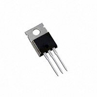
TO-220AB IRFB38N20DPbF
D2Pak IRFS38N20DPbF
TO-262 IRFSL38N20DPbF
Absolute Maximum Ratings
Parameter
ID @ TC = 25°C ID @ TC = 100°C IDM PD @TA = 25°C PD @TC = 25°C VGS dv/dt TJ TSTG Continuous Drain Current, VGS @ 10V Continuous Drain Current, VGS @ 10V Pulsed Drain Current Power Dissipation Power Dissipation Linear Derating Factor Gate-to-Source Voltage Peak Diode Recovery dv/dt Operating Junction and Storage Temperature Range Soldering Temperature, for 10 seconds Mounting torqe, 6-32 or M3 screw
Max.
38* 27* 180 3.8 230* 1.5* ± 30 9.5 -55 to + 175 300 (1.6mm from case ) 10 lbf•in (1.1N•m)
Units
A W W/°C V V/ns °C
Thermal Resistance
Parameter
RθJC RθCS RθJA RθJA Junction-to-Case Case-to-Sink, Flat, Greased Surface Junction-to-Ambient Junction-to-Ambient
Typ.
––– 0.50 ––– –––
Max.
0.47* ––– 62 40
Units
°C/W
* RθJC (end of life) for D2Pak and TO-262 = 0.50°C/W. This is the maximum measured value after 1000 temperature cycles from -55 to 150°C and is accounted for by the physical wearout of the die attach medium. Notes through are on page 11
www.irf.com
1
09/09/05
�PROVISIONAL
IRFB38N20DPbF/IRFS38N20DPbF/IRFSL38N20DPbF
Static @ TJ = 25°C (unless otherwise specified)
Parameter Drain-to-Source Breakdown Voltage ∆V(BR)DSS/∆TJ Breakdown Voltage Temp. Coefficient RDS(on) Static Drain-to-Source On-Resistance VGS(th) Gate Threshold Voltage V(BR)DSS IDSS IGSS Drain-to-Source Leakage Current Gate-to-Source Forward Leakage Gate-to-Source Reverse Leakage Min. 200 ––– ––– 3.0 ––– ––– ––– ––– Typ. ––– 0.22 ––– ––– ––– ––– ––– ––– Max. Units Conditions ––– V VGS = 0V, ID = 250µA ––– V/°C Reference to 25°C, ID = 1mA 0.054 Ω VGS = 10V, ID = 26A 5.0 V VDS = VGS, ID = 250µA 25 VDS = 200V, VGS = 0V µA 250 VDS = 160V, VGS = 0V, TJ = 150°C 100 VGS = 30V nA -100 VGS = -30V
Dynamic @ TJ = 25°C (unless otherwise specified)
gfs Qg Qgs Qgd td(on) tr td(off) tf Ciss Coss Crss Coss Coss Coss eff. Parameter Forward Transconductance Total Gate Charge Gate-to-Source Charge Gate-to-Drain ("Miller") Charge Turn-On Delay Time Rise Time Turn-Off Delay Time Fall Time Input Capacitance Output Capacitance Reverse Transfer Capacitance Output Capacitance Output Capacitance Effective Output Capacitance Min. 17 ––– ––– ––– ––– ––– ––– ––– ––– ––– ––– ––– ––– ––– Typ. ––– 60 17 28 16 95 29 47 2900 450 73 3550 180 380 Max. Units Conditions ––– S VDS = 50V, ID = 26A 91 ID = 26A 25 nC VDS = 100V 42 VGS = 10V, ––– VDD = 100V ––– ID = 26A ns ––– R G = 2.5Ω ––– VGS = 10V ––– VGS = 0V ––– VDS = 25V ––– pF ƒ = 1.0MHz ––– VGS = 0V, VDS = 1.0V, ƒ = 1.0MHz ––– VGS = 0V, VDS = 160V, ƒ = 1.0MHz ––– VGS = 0V, VDS = 0V to 160V
Avalanche Characteristics
Parameter EAS IAR EAR VDS (Avalanche) Single Pulse Avalanche Energy Avalanche Current
Repetitive Avalanche Voltage
Repetitive Avalanche Energy
Parameter Continuous Source Current (Body Diode) Pulsed Source Current (Body Diode) Diode Forward Voltage Reverse Recovery Time Reverse RecoveryCharge Forward Turn-On Time
Ã
dh
Min. ––– ––– ––– 260
Min. Typ. Max. Units
Typ. ––– ––– 390 –––
Max. 460 26 ––– –––
Units mJ A mJ V
Diode Characteristics
IS
ISM
VSD trr Qrr ton
Conditions D MOSFET symbol 44 ––– ––– showing the A G integral reverse ––– ––– 180 S p-n junction diode. ––– ––– 1.5 V TJ = 25°C, IS = 26A, VGS = 0V ––– 160 240 nS TJ = 25°C, IF = 26A ––– 1.3 2.0 µC di/dt = 100A/µs Intrinsic turn-on time is negligible (turn-on is dominated by LS+LD)
2
www.irf.com
�PROVISIONAL
IRFB38N20DPbF/IRFS38N20DPbF/IRFSL38N20DPbF
1000
100
ID, Drain-to-Source Current (A)
ID, Drain-to-Source Current (A)
VGS 15V 12V 10V 8.0V 7.0V 6.0V 5.5V BOTTOM 5.0V TOP
100
10
VGS 15V 12V 10V 8.0V 7.0V 6.0V 5.5V BOTTOM 5.0V TOP
5.0V
10
1
1
5.0V 300µs PULSE WIDTH Tj = 25°C
0.1 0.1 1 10 100
0.1 0.1 1
300µs PULSE WIDTH Tj = 175°C
10 100
VDS, Drain-to-Source Voltage (V)
VDS, Drain-to-Source Voltage (V)
Fig 1. Typical Output Characteristics
Fig 2. Typical Output Characteristics
1000.00
3.5
I D = 44A
ID, Drain-to-Source Current (Α )
3.0
RDS(on) , Drain-to-Source On Resistance
T J = 25°C T J = 175°C
2.5
100.00
(Normalized)
2.0
1.5
10.00
1.0
VDS = 15V
1.00 5.0 7.0 9.0
0.5
300µs PULSE WIDTH
11.0 13.0 15.0
0.0 -60 -40 -20 0 20 40 60 80
V GS = 10V
100 120 140 160 180
VGS, Gate-to-Source Voltage (V)
TJ , Junction Temperature
( ° C)
Fig 3. Typical Transfer Characteristics
Fig 4. Normalized On-Resistance Vs. Temperature
www.irf.com
3
�PROVISIONAL
IRFB38N20DPbF/IRFS38N20DPbF/IRFSL38N20DPbF
100000
VGS, Gate-to-Source Voltage (V)
VGS = 0V, f = 1 MHZ Ciss = C + Cgd, C gs ds SHORTED Crss = C gd Coss = C + C ds gd
12 10 8 6 4 2 0
ID = 26A VDS = 160V VDS = 100V
10000
C, Capacitance(pF)
Ciss
1000
Coss
100
Crss
10 1 10 100 1000
0
10
20
30
40
50
60
70
VDS, Drain-to-Source Voltage (V)
QG Total Gate Charge (nC)
Fig 5. Typical Capacitance Vs. Drain-to-Source Voltage
Fig 6. Typical Gate Charge Vs. Gate-to-Source Voltage
1000.00
1000
OPERATION IN THIS AREA LIMITED BY R DS (on)
100.00
T J = 175°C
ID, Drain-to-Source Current (A)
ISD, Reverse Drain Current (A)
100
100µsec 10 1msec 1 Tc = 25°C Tj = 175°C Single Pulse 1 10 100
10.00 T J = 25°C 1.00 VGS = 0V 0.10 0.0 0.5 1.0 1.5 2.0 2.5 VSD, Source-toDrain Voltage (V)
10msec
0.1
1000
VDS , Drain-toSource Voltage (V)
Fig 7. Typical Source-Drain Diode Forward Voltage
Fig 8. Maximum Safe Operating Area
4
www.irf.com
�PROVISIONAL
IRFB38N20DPbF/IRFS38N20DPbF/IRFSL38N20DPbF
50
V DS VGS
RD
40
RG 10V
Pulse Width ≤ 1 µs Duty Factor ≤ 0.1 %
D.U.T.
+
-VDD
ID , Drain Current (A)
30
20
Fig 10a. Switching Time Test Circuit
10
VDS 90%
0 25 50 75 100 125 150 175
TC , Case Temperature
( ° C)
Fig 9. Maximum Drain Current Vs. Case Temperature
10% VGS
td(on) tr t d(off) tf
Fig 10b. Switching Time Waveforms
1
(Z thJC )
D = 0.50
0.1
0.20 0.10
Thermal Response
0.05 0.02 0.01 0.01 SINGLE PULSE (THERMAL RESPONSE)
P DM t1 t2 Notes: 1. Duty factor D = 2. Peak T t1 / t 2 +TC 1
J = P DM x Z thJC
0.001 0.00001
0.0001
0.001
0.01
0.1
t1, Rectangular Pulse Duration (sec)
Fig 11. Maximum Effective Transient Thermal Impedance, Junction-to-Case
www.irf.com
5
�PROVISIONAL
IRFB38N20DPbF/IRFS38N20DPbF/IRFSL38N20DPbF
15V
900
TOP
RG
20V
D.U.T
IAS tp
+ V - DD
EAS , Single Pulse Avalanche Energy (mJ)
VDS
L
DRIVER
720
BOTTOM
ID 11A 19A 26A
540
A
0.01Ω
360
Fig 12a. Unclamped Inductive Test Circuit
180
V(BR)DSS tp
0 25 50 75 100 125 150 175
Starting Tj, Junction Temperature
( °C)
I AS
Fig 12c. Maximum Avalanche Energy Vs. Drain Current
Fig 12b. Unclamped Inductive Waveforms
Current Regulator Same Type as D.U.T.
QG
50KΩ 12V .2µF .3µF
10 V
QGS
QGD
VGS
3mA
D.U.T.
+ V - DS
VG
Charge
IG
ID
Current Sampling Resistors
Fig 13a. Basic Gate Charge Waveform
Fig 13b. Gate Charge Test Circuit
6
www.irf.com
�PROVISIONAL
IRFB38N20DPbF/IRFS38N20DPbF/IRFSL38N20DPbF
Peak Diode Recovery dv/dt Test Circuit
D.U.T
+
+
Circuit Layout Considerations • Low Stray Inductance • Ground Plane • Low Leakage Inductance Current Transformer
-
+
RG • • • • dv/dt controlled by RG Driver same type as D.U.T. ISD controlled by Duty Factor "D" D.U.T. - Device Under Test
+ VDD
Driver Gate Drive P.W. Period D=
P.W. Period VGS=10V
*
D.U.T. ISD Waveform Reverse Recovery Current Body Diode Forward Current di/dt D.U.T. VDS Waveform Diode Recovery dv/dt
VDD
Re-Applied Voltage Inductor Curent
Body Diode
Forward Drop
Ripple ≤ 5%
ISD
* VGS = 5V for Logic Level Devices Fig 14. For N-Channel HEXFET® Power MOSFETs
www.irf.com
7
�PROVISIONAL
IRFB38N20DPbF/IRFS38N20DPbF/IRFSL38N20DPbF
TO-220AB Package Outline
Dimensions are shown in millimeters (inches)
TO-220AB Part Marking Information
@Y6HQG@) UCDTÃDTÃ6IÃDSA � �à GPUÃ8P9@à &'( 6TT@H7G@9ÃPIÃXXà (�à ((& DIÃUC@Ã6TT@H7G`ÃGDI@ÃÅ8Å Ir)ÃÅQÅÃvhriyÃyvrÃvv vqvphrÃÅGrhqÃ�ÃA
rrÅ DIU@SI6UDPI6G S@8UDAD@S GPBP 6TT@H7G` GPUÃ8P9@ Q6SUÃIVH7@S 96U@Ã8P9@ `@6SÃ&Ã2Ã ((& X@@FÃ ( GDI@Ã8
8
www.irf.com
�PROVISIONAL
IRFB38N20DPbF/IRFS38N20DPbF/IRFSL38N20DPbF
D2Pak Package Outline
Dimensions are shown in millimeters (inches)
D2Pak Part Marking Information
UCDTÃDTÃ6IÃDSA$"�TÃXDUC GPUÃ8P9@Ã'�!# 6TT@H7G@9ÃPIÃXXÃ�!�Ã!��� DIÃUC@Ã6TT@H7G`ÃGDI@ÃÅGÅ DIU@SI6UDPI6G S@8UDAD@S GPBP 6TT@H7G` GPUÃ8P9@ Q6SUÃIVH7@S A$"�T 96U@Ã8P9@ `@6SÃ�Ã2Ã!��� X@@FÃ�! GDI@ÃG
25
DIU@SI6UDPI6G S@8UDAD@S GPBP 6TT@H7G` GPUÃ8P9@ A$"�T
Q6SUÃIVH7@S 96U@Ã8P9@ QÃ2Ã9@TDBI6U@TÃG@69Ã�ÃAS@@ QSP9V8UÃ�PQUDPI6G� `@6SÃ�Ã2Ã!��� X@@FÃ�! 6Ã2Ã6TT@H7G`ÃTDU@Ã8P9@
www.irf.com
9
�PROVISIONAL
IRFB38N20DPbF/IRFS38N20DPbF/IRFSL38N20DPbF
TO-262 Package Outline
Dimensions are shown in millimeters (inches)
IGBT 1- GATE
TO-262 Part Marking Information
@Y6HQG@) UCDTÃDTÃ6IÃDSG" �"G GPUÃ8P9@à &'( 6TT@H7G@9ÃPIÃXXà (�à ((& DIÃUC@Ã6TT@H7G`ÃGDI@ÃÅ8Å DIU@SI6UDPI6G S@8UDAD@S GPBP 6TT@H7G` GPUÃ8P9@ Q6SUÃIVH7@S
96U@Ã8P9@ `@6SÃ&Ã2Ã ((& X@@FÃ ( GDI@Ã8
25
DIU@SI6UDPI6G S@8UDAD@S GPBP 6TT@H7G` GPUÃ8P9@ Q6SUÃIVH7@S
96U@Ã8P9@ QÃ2Ã9@TDBI6U@TÃG@69�AS@@ QSP9V8UÃ�PQUDPI6G� `@6SÃ&Ã2à ((& X@@Fà ( 6Ã2Ã6TT@H7G`ÃTDU@Ã8P9@
10
www.irf.com
�PROVISIONAL
IRFB38N20DPbF/IRFS38N20DPbF/IRFSL38N20DPbF
D2Pak Tape & Reel Information
TRR
1.60 (.063) 1.50 (.059) 4.10 (.161) 3.90 (.153)
1.60 (.063) 1.50 (.059) 0.368 (.0145) 0.342 (.0135)
FEED DIRECTION 1.85 (.073)
1.65 (.065)
11.60 (.457) 11.40 (.449)
15.42 (.609) 15.22 (.601)
24.30 (.957) 23.90 (.941)
TRL
10.90 (.429) 10.70 (.421) 1.75 (.069) 1.25 (.049) 16.10 (.634) 15.90 (.626) 4.72 (.136) 4.52 (.178)
FEED DIRECTION
13.50 (.532) 12.80 (.504)
27.40 (1.079) 23.90 (.941)
4
330.00 (14.173) MAX.
60.00 (2.362) MIN.
Notes:
NOTES : 1. COMFORMS TO EIA-418. 2. CONTROLLING DIMENSION: MILLIMETER. 3. DIMENSION MEASURED @ HUB. 4. INCLUDES FLANGE DISTORTION @ OUTER EDGE.
26.40 (1.039) 24.40 (.961) 3
30.40 (1.197) MAX. 4
Repetitive rating; pulse width limited by
Coss eff. is a fixed capacitance that gives the same charging time max. junction temperature. as Coss while VDS is rising from 0 to 80% VDSS . Starting TJ = 25°C, L = 1.3mH This is only applied to TO-220AB package. RG = 25Ω, IAS = 26A. This is applied to D2Pak, when mounted on 1" square PCB ISD ≤ 26A, di/dt ≤ 390A/µs, VDD ≤ V(BR)DSS, (FR-4 or G-10 Material ). For recommended footprint and soldering TJ ≤ 175°C. techniques refer to application note #AN-994. Pulse width ≤ 300µs; duty cycle ≤ 2%.
TO-220 package is not recommended for Surface Mount Application.
Data and specifications subject to change without notice. This product has been designed and qualified for the Automotive [Q101] (IRFB38N20DPbF), & Industrial (IRFS38N20DPbF/IRFSL38N20D) market. Qualification Standards can be found on IR’s Web site.
IR WORLD HEADQUARTERS: 233 Kansas St., El Segundo, California 90245, USA Tel: (310) 252-7105 TAC Fax: (310) 252-7903 Visit us at www.irf.com for sales contact information.09/05
www.irf.com
11
�