PD - 91817A
SMPS MOSFET
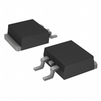
IRFS9N60A
HEXFET® Power MOSFET
Applications l Switch Mode Power Supply ( SMPS ) l Uninterruptable Power Supply l High Speed Power Switching Benefits Low Gate Charge Qg results in Simple Drive Requirement l Improved Gate, Avalanche and dynamic dv/dt Ruggedness l Fully Characterized Capacitance and Avalanche Voltage and Current
l
VDSS
600V
RDS(on) max
0.75Ω
ID
9.2A
GDS
D2Pak
Absolute Maximum Ratings
Parameter
ID @ TC = 25°C ID @ TC = 100°C IDM PD @TC = 25°C VGS dv/dt TJ TSTG Continuous Drain Current, VGS @ 10V Continuous Drain Current, VGS @ 10V Pulsed Drain Current Power Dissipation Linear Derating Factor Gate-to-Source Voltage Peak Diode Recovery dv/dt Operating Junction and Storage Temperature Range Soldering Temperature, for 10 seconds
Max.
9.2 5.8 37 170 1.3 ± 30 5.0 -55 to + 150 300 (1.6mm from case )
Units
A W W/°C V V/ns °C
Applicable Off Line SMPS Topologies:
l l
Active Clamped Forward Main Switch
Notes through
are on page 9
www.irf.com
1
9/23/99
�IRFS9N60A
Static @ TJ = 25°C (unless otherwise specified)
V(BR)DSS
∆V(BR)DSS/∆TJ
RDS(on) VGS(th) IDSS IGSS
Parameter Drain-to-Source Breakdown Voltage Breakdown Voltage Temp. Coefficient Static Drain-to-Source On-Resistance Gate Threshold Voltage Drain-to-Source Leakage Current Gate-to-Source Forward Leakage Gate-to-Source Reverse Leakage
Min. Typ. Max. Units Conditions 600 ––– ––– V VGS = 0V, ID = 250µA ––– 0.66 ––– V/°C Reference to 25°C, ID = 1mA ––– ––– 0.75 Ω VGS = 10V, ID = 5.5.A 2.0 ––– 4.0 V VDS = VGS, ID = 250µA ––– ––– 25 VDS = 600V, VGS = 0V µA ––– ––– 250 VDS = 480V, VGS = 0V, T J = 125°C ––– ––– 100 VGS = 30V nA ––– ––– -100 VGS = -30V
Dynamic @ TJ = 25°C (unless otherwise specified)
gfs Qg Qgs Qgd td(on) tr td(off) tf Ciss Coss Crss Coss Coss Coss eff. Parameter Forward Transconductance Total Gate Charge Gate-to-Source Charge Gate-to-Drain ("Miller") Charge Turn-On Delay Time Rise Time Turn-Off Delay Time Fall Time Input Capacitance Output Capacitance Reverse Transfer Capacitance Output Capacitance Output Capacitance Effective Output Capacitance Min. 5.5 ––– ––– ––– ––– ––– ––– ––– ––– ––– ––– ––– ––– ––– Typ. ––– ––– ––– ––– 13 25 30 22 1400 180 7.1 1957 49 96 Max. Units Conditions ––– S VDS = 25V, ID = 3.1A 49 ID = 9.2A 13 nC VDS = 400V 20 VGS = 10V, See Fig. 6 and 13 ––– VDD = 300V ––– ID = 9.2A ns ––– RG = 9.1Ω ––– R D = 35.5Ω,See Fig. 10 ––– VGS = 0V ––– VDS = 25V ––– pF ƒ = 1.0MHz, See Fig. 5 ––– VGS = 0V, VDS = 1.0V, ƒ = 1.0MHz ––– VGS = 0V, VDS = 480V, ƒ = 1.0MHz ––– VGS = 0V, VDS = 0V to 480V
Avalanche Characteristics
Parameter
EAS IAR EAR Single Pulse Avalanche Energy Avalanche Current Repetitive Avalanche Energy
Typ.
––– ––– –––
Max.
290 9.2 17
Units
mJ A mJ
Thermal Resistance
Parameter
RθJC RθJA Junction-to-Case Junction-to-Ambient (PCB Mounted,steady-state) Parameter Continuous Source Current (Body Diode) Pulsed Source Current (Body Diode) Diode Forward Voltage Reverse Recovery Time Reverse RecoveryCharge Forward Turn-On Time
Typ.
––– –––
Max.
0.75 40
Units
°C/W
Diode Characteristics
Min. Typ. Max. Units IS
ISM
VSD trr Qrr ton
Conditions D MOSFET symbol ––– ––– 9.2 showing the A G integral reverse ––– ––– 37 S p-n junction diode. ––– ––– 1.5 V TJ = 25°C, IS = 9.2A, VGS = 0V ––– 530 800 ns TJ = 25°C, IF = 9.2A ––– 3.0 4.4 µC di/dt = 100A/µs Intrinsic turn-on time is negligible (turn-on is dominated by LS+LD)
2
www.irf.com
�IRFS9N60A
100
VGS 15V 10V 8.0V 7.0V 6.0V 5.5V 5.0V BOTTOM 4.7V TOP
100
I D , Drain-to-Source Current (A)
10
I D , Drain-to-Source Current (A)
VGS 15V 10V 8.0V 7.0V 6.0V 5.5V 5.0V BOTTOM 4.7V TOP
10
1
4.7V
20µs PULSE WIDTH TJ = 25 °C
1 10 100
4.7V
20µs PULSE WIDTH TJ = 150 °C
1 10 100
0.1 0.1
1
VDS , Drain-to-Source Voltage (V)
VDS , Drain-to-Source Voltage (V)
Fig 1. Typical Output Characteristics
Fig 2. Typical Output Characteristics
100
3.0
ID = 9.2A
RDS(on) , Drain-to-Source On Resistance (Normalized)
I D , Drain-to-Source Current (A)
2.5
10
TJ = 150 ° C
2.0
1.5
TJ = 25 ° C
1
1.0
0.5
0.1 4.0
V DS = 50V 20µs PULSE WIDTH 5.0 6.0 7.0 8.0 9.0 10.0
0.0 -60 -40 -20
VGS = 10V
0 20 40 60 80 100 120 140 160
VGS , Gate-to-Source Voltage (V)
TJ , Junction Temperature ( °C)
Fig 3. Typical Transfer Characteristics
Fig 4. Normalized On-Resistance Vs. Temperature
www.irf.com
3
�IRFS9N60A
2400
20
2000
VGS , Gate-to-Source Voltage (V)
V GS C is s C rss C o ss
= = = =
0V, f = 1M H z C g s + C g d , Cd s S H O R TE D C gd C ds + C gd
ID = 9.2A
400V VDS = 480V VDS = 300V VDS = 120V
16
C , Capacitance (pF )
C i ss
1600
C o ss
1200
12
8
800
400
C r ss
4
0 1 10 100 1000
A
0 0 10 20
FOR TEST CIRCUIT SEE FIGURE 13
30 40 50
V D S , D rain-to-S ource V olta g e ( V )
Q G , Total Gate Charge (nC)
Fig 5. Typical Capacitance Vs. Drain-to-Source Voltage
Fig 6. Typical Gate Charge Vs. Gate-to-Source Voltage
100
1000
OPERATION IN THIS AREA LIMITED BY RDS(on)
ISD , Reverse Drain Current (A)
10
I D , Drain Current (A)
100
TJ = 150 ° C
10us 10 100us 1ms 1 10ms
1
TJ = 25 ° C
0.1 0.2
V GS = 0 V
0.5 0.7 1.0 1.2
0.1
TC = 25 ° C TJ = 150 ° C Single Pulse
10 100 1000 10000
VSD ,Source-to-Drain Voltage (V)
VDS , Drain-to-Source Voltage (V)
Fig 7. Typical Source-Drain Diode Forward Voltage
Fig 8. Maximum Safe Operating Area
4
www.irf.com
�IRFS9N60A
10.0
VDS VGS
RD
8.0
D.U.T.
+
RG
I D , Drain Current (A)
-VDD
6.0
10V
Pulse Width ≤ 1 µs Duty Factor ≤ 0.1 %
4.0
Fig 10a. Switching Time Test Circuit
2.0
VDS 90%
0.0 25 50 75 100 125 150
TC , Case Temperature
( °C)
10% VGS
Fig 9. Maximum Drain Current Vs. Case Temperature
td(on)
tr
t d(off)
tf
Fig 10b. Switching Time Waveforms
1
Thermal Response (Z thJC )
D = 0.50
0.20 0.1
0.10 0.05 0.02 0.01 P DM t1 SINGLE PULSE (THERMAL RESPONSE) t2 Notes: 1. Duty factor D = t 1 / t 2 2. Peak T J = P DM x Z thJC + TC 0.001 0.01 0.1 1
0.01 0.00001
0.0001
t1 , Rectangular Pulse Duration (sec)
Fig 11. Maximum Effective Transient Thermal Impedance, Junction-to-Case
www.irf.com
5
�IRFS9N60A
600
EAS , Single Pulse Avalanche Energy (mJ)
TOP
500
1 5V
BOTTOM
ID 4.1A 5.8A 9.2A
VDS
L
D R IV E R
400
RG
20V tp
D .U .T
IA S
300
+ V - DD
A
0 .0 1 Ω
200
Fig 12a. Unclamped Inductive Test Circuit
100
0 25 50 75 100 125 150
V (B R )D SS tp
Starting TJ , Junction Temperature ( °C)
Fig 12c. Maximum Avalanche Energy Vs. Drain Current
IAS
Fig 12b. Unclamped Inductive Waveforms
Current Regulator Same Type as D.U.T.
50KΩ
QG
12V
.2µF
.3µF
10 V
QGS VG QGD
VGS
3mA
D.U.T.
+ V - DS
Charge
IG
ID
Current Sampling Resistors
Fig 13a. Basic Gate Charge Waveform
Fig 13b. Gate Charge Test Circuit
6
www.irf.com
�IRFS9N60A
Peak Diode Recovery dv/dt Test Circuit
D.U.T
+
+
Circuit Layout Considerations • Low Stray Inductance • Ground Plane • Low Leakage Inductance Current Transformer
-
+
RG • • • • dv/dt controlled by RG Driver same type as D.U.T. ISD controlled by Duty Factor "D" D.U.T. - Device Under Test
+ VDD
Driver Gate Drive P.W. Period D=
P.W. Period VGS=10V
*
D.U.T. ISD Waveform Reverse Recovery Current Body Diode Forward Current di/dt D.U.T. VDS Waveform Diode Recovery dv/dt
VDD
Re-Applied Voltage Inductor Curent
Body Diode
Forward Drop
Ripple ≤ 5%
ISD
* VGS = 5V for Logic Level Devices Fig 14. For N-Channel HEXFET® Power MOSFETs
www.irf.com
7
�IRFS9N60A
D2Pak Package Outline
1 0.54 (.4 15) 1 0.29 (.4 05) 1.4 0 (.055 ) M AX. -A2
4.69 (.1 85) 4.20 (.1 65)
-B 1.3 2 (.05 2) 1.2 2 (.04 8)
1 0.16 (.4 00 ) RE F.
6.47 (.2 55 ) 6.18 (.2 43 ) 15 .4 9 (.6 10) 14 .7 3 (.5 80) 5 .28 (.20 8) 4 .78 (.18 8) 2.7 9 (.110 ) 2.2 9 (.090 ) 2.61 (.1 03 ) 2.32 (.0 91 ) 1.3 9 (.0 5 5) 1.1 4 (.0 4 5) 8.8 9 (.3 50 ) R E F.
1.7 8 (.07 0) 1.2 7 (.05 0)
1
3
3X
1.40 (.0 55) 1.14 (.0 45) 3X 5 .08 (.20 0)
0 .93 (.03 7 ) 0 .69 (.02 7 ) 0 .25 (.01 0 ) M BAM
0.5 5 (.022 ) 0.4 6 (.018 )
M IN IM U M R E CO M M E ND E D F O O TP R IN T 1 1.43 (.4 50 )
NO TE S: 1 D IM EN S IO N S A FTER SO L D ER D IP. 2 D IM EN S IO N IN G & TO LE RA N C IN G PE R A N S I Y1 4.5M , 198 2. 3 C O N TRO L LIN G D IM EN SIO N : IN C H . 4 H E ATSINK & L EA D D IM EN S IO N S D O N O T IN C LU D E B UR R S.
LE A D A SS IG N M E N TS 1 - G A TE 2 - D R AIN 3 - S O U RC E
8.89 (.3 50 ) 17 .78 (.70 0)
3 .8 1 (.15 0) 2 .08 (.08 2) 2X 2.5 4 (.100 ) 2X
Part Marking Information
D2Pak
IN TE R N A TIO N A L R E C T IF IE R LO G O A S S E M B LY LO T C O D E
PART NUM BER F530S 9 24 6 9B 1M
A
DATE CODE (Y YW W ) YY = Y E A R W W = W EEK
8
www.irf.com
�IRFS9N60A
Tape & Reel Information
D2Pak
TR R
1 .6 0 (.0 63 ) 1 .5 0 (.0 59 ) 4 .1 0 ( .1 6 1) 3 .9 0 ( .1 5 3)
1.60 (.06 3) 1.50 (.05 9) 0 .3 68 (.0 145 ) 0 .3 42 (.0 135 )
F E ED D IRE C TIO N 1 .8 5 (.0 7 3 )
1 .6 5 (.0 6 5 )
1 1.60 (.457 ) 1 1.40 (.449 )
15 .4 2 (.60 9) 15 .2 2 (.60 1)
24.30 (.95 7) 23.90 (.94 1)
TR L
10 .9 0 (.42 9) 10 .7 0 (.42 1) 1.75 (.0 69 ) 1.25 (.0 49 ) 16 .1 0 (.63 4) 15 .9 0 (.62 6) 4 .7 2 (.13 6) 4 .5 2 (.17 8)
F E ED D IR E CT IO N
13.50 (.532) 12.80 (.504)
27.40 (1.079) 23.90 (.941) 4
33 0.00 (14.173) M AX .
60.00 (2.362) M IN.
NO TE S : 1. CO MF OR M S TO EIA-418. 2. CO N TRO LLIN G DIM ENSIO N : MILLIM ET ER . 3. DIM ENS ION MEAS URED @ HU B. 4. INC LUD ES FLAN GE DIS TO RTIO N @ OU TER ED G E.
30.40 (1.197) MA X. 26.40 (1.039) 24.40 (.961)
4
3
Notes:
Repetitive rating; pulse width limited by
max. junction temperature. ( See fig. 11 )
Pulse width ≤ 300µs; duty cycle ≤ 2%.
Coss eff. is a fixed capacitance that gives the same charging time
as Coss while VDS is rising from 0 to 80% VDSS
Starting TJ = 25°C, L = 6.8mH
RG = 25Ω, IAS = 9.2A. (See Figure 12)
ISD ≤ 9.2A, di/dt ≤ 50A/µs, VDD ≤ V(BR)DSS,
TJ ≤ 150°C
WORLD HEADQUARTERS: 233 Kansas St., El Segundo, California 90245, Tel: (310) 322 3331 IR GREAT BRITAIN: Hurst Green, Oxted, Surrey RH8 9BB, UK Tel: ++ 44 1883 732020 IR CANADA: 15 Lincoln Court, Brampton, Ontario L6T3Z2, Tel: (905) 453 2200 IR GERMANY: Saalburgstrasse 157, 61350 Bad Homburg Tel: ++ 49 6172 96590 IR ITALY: Via Liguria 49, 10071 Borgaro, Torino Tel: ++ 39 11 451 0111 IR FAR EAST: K&H Bldg., 2F, 30-4 Nishi-Ikebukuro 3-Chome, Toshima-Ku, Tokyo Japan 171 Tel: 81 3 3983 0086 IR SOUTHEAST ASIA: 1 Kim Seng Promenade, Great World City West Tower, 13-11, Singapore 237994 Tel: ++ 65 838 4630 IR TAIWAN:16 Fl. Suite D. 207, Sec. 2, Tun Haw South Road, Taipei, 10673, Taiwan Tel: 886-2-2377-9936 http://www.irf.com/ Data and specifications subject to change without notice. 9/99
www.irf.com
9
�