PD - 95429
IRG4BC40WPbF
INSULATED GATE BIPOLAR TRANSISTOR
Features
Designed expressly for Switch-Mode Power Supply and PFC (power factor correction) applications Industry-benchmark switching losses improve efficiency of all power supply topologies 50% reduction of Eoff parameter Low IGBT conduction losses Latest-generation IGBT design and construction offers tighter parameters distribution, exceptional reliability Lead-Free
C
VCES = 600V
G E
VCE(on) typ. = 2.05V
@VGE = 15V, IC = 20A
n-channel
Benefits
Lower switching losses allow more cost-effective operation than power MOSFETs up to 150 kHz ("hard switched" mode) Of particular benefit to single-ended converters and boost PFC topologies 150W and higher Low conduction losses and minimal minority-carrier recombination make these an excellent option for resonant mode switching as well (up to >>300 kHz)
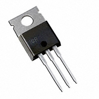
TO-220AB
Absolute Maximum Ratings
Parameter
VCES IC @ TC = 25°C IC @ TC = 100°C ICM ILM VGE EARV PD @ TC = 25°C PD @ TC = 100°C TJ TSTG Collector-to-Emitter Breakdown Voltage Continuous Collector Current Continuous Collector Current Pulsed Collector Current Clamped Inductive Load Current Gate-to-Emitter Voltage Reverse Voltage Avalanche Energy Maximum Power Dissipation Maximum Power Dissipation Operating Junction and Storage Temperature Range Soldering Temperature, for 10 seconds Mounting torque, 6-32 or M3 screw.
Max.
600 40 20 160 160 ± 20 160 160 65 -55 to + 150 300 (0.063 in. (1.6mm) from case ) 10 lbfin (1.1Nm)
Units
V A
V mJ W °C
Thermal Resistance
Parameter
RθJC RθCS RθJA Wt Junction-to-Case Case-to-Sink, Flat, Greased Surface Junction-to-Ambient, typical socket mount Weight
Typ.
0.5 2.0 (0.07)
Max.
0.77 80
Units
°C/W g (oz)
www.irf.com
1
06/17/04
�IRG4BC40WPbF
Electrical Characteristics @ TJ = 25°C (unless otherwise specified)
Parameter Min. Typ. Max. Units Conditions Collector-to-Emitter Breakdown Voltage 600 V VGE = 0V, IC = 250µA Emitter-to-Collector Breakdown Voltage 18 V VGE = 0V, IC = 1.0A ∆V(BR)CES/∆TJ Temperature Coeff. of Breakdown Voltage 0.44 V/°C VGE = 0V, IC = 1.0mA 2.05 2.5 IC = 20A VGE = 15V VCE(ON) Collector-to-Emitter Saturation Voltage 2.36 IC = 40A See Fig.2, 5 V 1.90 IC = 20A , TJ = 150°C VGE(th) Gate Threshold Voltage 3.0 6.0 VCE = VGE, IC = 250µA ∆V GE(th)/∆TJ Temperature Coeff. of Threshold Voltage 13 mV/°C VCE = VGE, IC = 250µA gfe Forward Transconductance
18 28 S VCE = 100 V, IC =20A 250 VGE = 0V, VCE = 600V ICES Zero Gate Voltage Collector Current µA 2.0 VGE = 0V, VCE = 10V, TJ = 25°C 2500 VGE = 0V, VCE = 600V, TJ = 150°C IGES Gate-to-Emitter Leakage Current ±100 nA VGE = ±20V V(BR)CES V(BR)ECS
Switching Characteristics @ TJ = 25°C (unless otherwise specified)
Qg Qge Qgc t d(on) tr td(off) tf Eon Eoff E ts td(on) tr td(off) tf Ets LE Cies Coes Cres Notes: Parameter Total Gate Charge (turn-on) Gate - Emitter Charge (turn-on) Gate - Collector Charge (turn-on) Turn-On Delay Time Rise Time Turn-Off Delay Time Fall Time Turn-On Switching Loss Turn-Off Switching Loss Total Switching Loss Turn-On Delay Time Rise Time Turn-Off Delay Time Fall Time Total Switching Loss Internal Emitter Inductance Input Capacitance Output Capacitance Reverse Transfer Capacitance Min. Typ. 98 12 36 27 22 100 74 0.11 0.23 0.34 25 23 170 124 0.85 7.5 1900 140 35 Max. Units Conditions 147 IC =20A 18 nC VCC = 400V See Fig.8 54 VGE = 15V TJ = 25°C ns 150 IC = 20A, VCC = 480V 110 VGE = 15V, RG = 10 Ω Energy losses include "tail" mJ See Fig. 9,10, 14 0.45 TJ = 150°C, IC = 20A, VCC = 480V ns VGE = 15V, RG = 10 Ω Energy losses include "tail" mJ See Fig. 10,11, 14 nH Measured 5mm from package VGE = 0V pF VCC = 30V See Fig. 7 = 1.0MHz
Repetitive rating; VGE = 20V, pulse width limited by
max. junction temperature. ( See fig. 13b )
VCC = 80%(VCES), VGE = 20V, L = 10µH, RG = 10Ω,
(See fig. 13a)
Pulse width ≤ 80µs; duty factor ≤ 0.1%.
Pulse width 5.0µs, single shot.
Repetitive rating; pulse width limited by maximum
junction temperature.
2
www.irf.com
�IRG4BC40WPbF
50
For both:
Triangular wave:
40
Load Current ( A )
Duty cycle: 50% TJ = 125°C Tsink = 90°C Gate drive as specified Power Dissipation = 28W
Clamp voltage: 80% of rated
30 Square wave: 60% of rated voltage
20
10 Ideal diodes
0 0.1 1 10 100
A
1000
f, Frequency (kHz)
Fig. 1 - Typical Load Current vs. Frequency
(Load Current = IRMS of fundamental)
1000
1000
I C , Collector-to-Emitter Current (A)
TJ = 25 ° C
100
I C , Collector-to-Emitter Current (A)
100
TJ = 150 °C
TJ = 150 °C
10
10
TJ = 25 °C
1 1.0
V GE = 15V 80µs PULSE WIDTH
2.0 3.0 4.0 5.0
1 5 7
V CC = 50V 5µs PULSE WIDTH
9 11
VCE , Collector-to-Emitter Voltage (V)
VGE , Gate-to-Emitter Voltage (V)
Fig. 2 - Typical Output Characteristics
Fig. 3 - Typical Transfer Characteristics
www.irf.com
3
�IRG4BC40WPbF
50
3.0
VCE , Collector-to-Emitter Voltage(V)
VGE = 15V 80 us PULSE WIDTH IC = 40 A
Maximum DC Collector Current(A)
40
2.5
30
2.0
IC = 20 A IC = 10 A
20
1.5
10
0
25
50
75
100
125
150
1.0 -60 -40 -20
0
20
40
60
80 100 120 140 160
TC , Case Temperature ( °C)
TJ , Junction Temperature ( ° C)
Fig. 4 - Maximum Collector Current vs. Case Temperature
Fig. 5 - Typical Collector-to-Emitter Voltage vs. Junction Temperature
1
Thermal Response (Z thJC )
D = 0.50
0.20 0.1 0.10 0.05 0.02 0.01 SINGLE PULSE (THERMAL RESPONSE) Notes: 1. Duty factor D = t 1 / t 2 2. Peak TJ = PDM x Z thJC + TC 0.001 0.01 0.1 1 PDM t1 t2
0.01 0.00001
0.0001
t1 , Rectangular Pulse Duration (sec)
Fig. 6 - Maximum Effective Transient Thermal Impedance, Junction-to-Case
4
www.irf.com
�IRG4BC40WPbF
4000
VGE , Gate-to-Emitter Voltage (V)
VGE = 0V, f = 1MHz Cies = Cge + Cgc , Cce SHORTED Cres = Cgc Coes = Cce + Cgc
20
VCC = 400V I C = 20A
16
C, Capacitance (pF)
3000
Cies
2000
12
8
Coes
1000
Cres
4
0 1 10 100
0 0 20 40 60 80 100
VCE , Collector-to-Emitter Voltage (V)
QG , Total Gate Charge (nC)
Fig. 7 - Typical Capacitance vs. Collector-to-Emitter Voltage
Fig. 8 - Typical Gate Charge vs. Gate-to-Emitter Voltage
1.0
0.8 0.7 0.6 0.5 0.4 0.3 10
Total Switching Losses (mJ)
Total Switching Losses (mJ)
V CC = 480V V GE = 15V 0.9 TJ = 25 °C I C = 20A
10
RG = 10 Ω 10Ohm VGE = 15V VCC = 480V
IC = 40 A
1
IC = 20 A IC = 10 A
RG , Gate Resistance (Ω) (Ohm)
20
30
40
50
60
0.1 -60 -40 -20
0
20
40
60
80 100 120 140 160
TJ , Junction Temperature ( °C )
Fig. 9 - Typical Switching Losses vs. Gate Resistance
Fig. 10 - Typical Switching Losses vs. Junction Temperature
www.irf.com
5
�IRG4BC40WPbF
2.0
1.5
1.0
I C, Collector-to-Emitter Current (A)
Total Switching Losses (mJ)
RG TJ VCC VGE
=10 Ω 10Ohm = 150 ° C = 480V = 15V
1000
VGE = 20V T J = 125 oC
100
0.5
0.0 5 15 25 35 45
SAFE OPERATING AREA
10 1 10 100 1000
I C , Collector-to-emitter Current (A)
VCE , Collector-to-Emitter Voltage (V)
Fig. 11 - Typical Switching Losses vs. Collector-to-Emitter Current
Fig. 12 - Turn-Off SOA
6
www.irf.com
�IRG4BC40WPbF
L 50V 1000V VC *
0 - 480V
D.U.T.
RL =
480V 4 X I C@25°C
c
480µF 960V
d
* Driver same type as D.U.T.; Vc = 80% of Vce(max) * Note: Due to the 50V power supply, pulse width and inductor will increase to obtain rated Id.
Fig. 13a - Clamped Inductive
Load Test Circuit
Fig. 13b - Pulsed Collector
Current Test Circuit
IC L Driver* 50V D.U.T. VC
Fig. 14a - Switching Loss
Test Circuit
* Driver same type as D.U.T., VC = 480V
Ã
1000V
d
e
c d
90%
e
VC 90%
10%
t d(off)
Fig. 14b - Switching Loss
Waveforms
10% I C 5% t d(on)
tr E on E ts = (Eon +Eoff )
tf t=5µs E off
www.irf.com
7
�IRG4BC40WPbF
TO-220AB Package Outline
Dimensions are shown in millimeters (inches)
10.54 (.415) 10.29 (.405) 3.78 (.149) 3.54 (.139) -A6.47 (.255) 6.10 (.240) -B4.69 (.185) 4.20 (.165) 1.32 (.052) 1.22 (.048)
2.87 (.113) 2.62 (.103)
4 15.24 (.600) 14.84 (.584)
LEAD ASSIGNMENTS
1.15 (.045) MIN 1 2 3 LEAD ASSIGNMENTS IGBTs, CoPACK 1 - GATE 21- GATE DRAIN 1- GATE 32- DRAINSOURCE 2- COLLECTOR 3- EMITTER 3- SOURCE 4 - DRAIN
HEXFET
14.09 (.555) 13.47 (.530)
4- DRAIN
4.06 (.160) 3.55 (.140)
4- COLLECTOR
3X 3X 1.40 (.055) 1.15 (.045)
0.93 (.037) 0.69 (.027) M BAM
3X
0.55 (.022) 0.46 (.018)
0.36 (.014)
2.54 (.100) 2X NOTES: 1 DIMENSIONING & TOLERANCING PER ANSI Y14.5M, 1982. 2 CONTROLLING DIMENSION : INCH
2.92 (.115) 2.64 (.104)
3 OUTLINE CONFORMS TO JEDEC OUTLINE TO-220AB. 4 HEATSINK & LEAD MEASUREMENTS DO NOT INCLUDE BURRS.
TO-220AB Part Marking Information
E XAMP L E : T H IS IS AN IR F 1010 L OT CODE 1789 AS S E MB L E D ON WW 19, 1997 IN T H E AS S E MB L Y L INE "C" INT E R NAT IONAL R E CT IF IE R L OGO AS S E MB L Y L OT CODE PAR T NU MB E R
Note: "P" in assembly line position indicates "Lead-Free"
DAT E CODE YE AR 7 = 1997 WE E K 19 L INE C
Data and specifications subject to change without notice.
IR WORLD HEADQUARTERS: 233 Kansas St., El Segundo, California 90245, USA Tel: (310) 252-7105 TAC Fax: (310) 252-7903 Visit us at www.irf.com for sales contact information. 06/04
8
www.irf.com
�Note: For the most current drawings please refer to the IR website at: http://www.irf.com/package/
�