PD -95891
IRG4BH20K-SPbF
INSULATED GATE BIPOLAR TRANSISTOR
Features
• High short circuit rating optimized for motor control, tsc =10µs @ VCC = 720V , TJ = 125°C, VGE = 15V • Combines low conduction losses with high switching speed • Latest generation design provides tighter parameter distribution and higher efficiency than previous generations • Industry standard D2Pak package • Lead-Free
C
Short Circuit Rated UltraFast IGBT
VCES = 1200V
G E
VCE(on) typ. = 3.17V
@VGE = 15V, IC = 5.0A
n-channel
Benefits
• As a Freewheeling Diode we recommend our HEXFREDTM ultrafast, ultrasoft recovery diodes for minimum EMI / Noise and switching losses in the Diode and IGBT • Latest generation 4 IGBT's offer highest power density motor controls possible
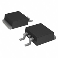
D2Pak
Absolute Maximum Ratings
Parameter
VCES IC @ TC = 25°C IC @ TC = 100°C ICM ILM tsc VGE EARV PD @ TC = 25°C PD @ TC = 100°C TJ TSTG Collector-to-Emitter Voltage Continuous Collector Current Continuous Collector Current Pulsed Collector Current Clamped Inductive Load Current Short Circuit Withstand Time Gate-to-Emitter Voltage Reverse Voltage Avalanche Energy Maximum Power Dissipation Maximum Power Dissipation Operating Junction and Storage Temperature Range
Max.
1200 11 5.0 22 22 10 ±20 130 60 24 -55 to +150
Units
V
A µs V mJ W °C
Thermal Resistance
Parameter
RθJC RθCS RθJA Wt Junction-to-Case Case-to-Sink, Flat, Greased Surface Junction-to-Ambient, typical socket mount Weight
Typ.
––– 0.24 ––– 6 (0.21)
Max.
2.1 ––– 40 –––
Units
°C/W g (oz)
www.irf.com
1
04/10/07
�IRG4BH20K-SPbF
Electrical Characteristics @ TJ = 25°C (unless otherwise specified)
V(BR)CES V(BR)ECS Parameter Min. Typ. Collector-to-Emitter Breakdown Voltage 1200 — Emitter-to-Collector Breakdown Voltage 18 — ∆V(BR)CES/∆TJ Temperature Coeff. of Breakdown Voltage — 1.13 — 3.17 VCE(ON) Collector-to-Emitter Saturation Voltage — 4.04 — 2.84 VGE(th) Gate Threshold Voltage 3.5 — ∆VGE(th)/∆TJ Temperature Coeff. of Threshold Voltage — -10 gfe Forward Transconductance
2.3 3.5 — — ICES Zero Gate Voltage Collector Current — — — — IGES Gate-to-Emitter Leakage Current — — Max. Units Conditions — V VGE = 0V, IC = 250µA — V VGE = 0V, IC = 1.0A — V/°C VGE = 0V, IC = 2.5mA 4.3 IC = 5.0A VGE = 15V — IC = 11A See Fig.2, 5 V — IC = 5.0A , TJ = 150°C 6.5 VCE = VGE, IC = 250µA — mV/°C VCE = VGE, IC = 1mA — S VCE = 100 V, IC = 5.0A 250 VGE = 0V, VCE = 1200V µA 2.0 VGE = 0V, VCE = 10V, TJ = 25°C 1000 VGE = 0V, VCE = 1200V, TJ = 150°C ±100 nA VGE = ±20V
Switching Characteristics @ TJ = 25°C (unless otherwise specified)
Qg Qge Qgc td(on) tr td(off) tf Eon Eoff Ets tsc td(on) tr td(off) tf Ets LE Cies Coes Cres Notes: Parameter Total Gate Charge (turn-on) Gate - Emitter Charge (turn-on) Gate - Collector Charge (turn-on) Turn-On Delay Time Rise Time Turn-Off Delay Time Fall Time Turn-On Switching Loss Turn-Off Switching Loss Total Switching Loss Short Circuit Withstand Time Turn-On Delay Time Rise Time Turn-Off Delay Time Fall Time Total Switching Loss Internal Emitter Inductance Input Capacitance Output Capacitance Reverse Transfer Capacitance Min. — — — — — — — — — — 10 — — — — — — — — — Typ. Max. Units Conditions 28 43 IC = 5.0A 4.4 6.6 nC VCC = 400V See Fig.8 12 18 VGE = 15V 23 — 26 — TJ = 25°C ns 93 140 IC =5.0A, VCC = 960V 270 400 VGE = 15V, RG = 50Ω 0.45 — Energy losses include "tail" 0.44 — mJ See Fig. 9,10,14 0.89 1.2 — — µs VCC = 720V, TJ = 125°C VGE = 15V, RG = 50Ω 23 — TJ = 150°C, 28 — IC = 5.0A, VCC = 960V ns 100 — VGE = 15V, RG = 50 Ω 620 — Energy losses include "tail" 1.7 — mJ See Fig. 10,11,14 7.5 — nH Between lead and center of die contact 435 — VGE = 0V 44 — pF VCC = 30V See Fig. 7 8.3 — ƒ = 1.0MHz
Repetitive rating; VGE = 20V, pulse width limited by
max. junction temperature. ( See fig. 13b ) (See fig. 13a)
Repetitive rating; pulse width limited by maximum
junction temperature.
VCC = 80%(VCES), VGE = 20V, L = 10µH, RG =50Ω,
Pulse width ≤ 80µs; duty factor ≤ 0.1%.
Pulse width 5.0µs, single shot. * When mounted on 1" square PCB (FR-4 or G-10 Material ). For recommended footprint and soldering techniques refer to application note #AN-994.
2
www.irf.com
�IRG4BH20K-SPbF
16
F or both:
Triangular wave:
Load Current ( A )
12
Duty cycle: 50% TJ = 125 ˚ C T sink = 90 ˚ C Gate drive as specified
Power Dissipation = 15W
Clamp voltage: 80% of rated
Sq uare wav e:
8
60% of rated voltage
4
Ideal diodes
0
)
0.1 1
f, Frequency (kHz)
10
100
Fig. 1 - Typical Load Current vs. Frequency
(Load Current = IRMS of fundamental)
100
100
I C , Collector-to-Emitter Current (A)
10
TJ = 150 °C
I C , Collector-to-Emitter Current (A)
10
TJ = 150 °C
1
TJ = 25 °C V GE = 15V 20µs PULSE WIDTH
1 10
TJ = 25 °C V CC = 50V 5µs PULSE WIDTH
6 8 10 12 14
0.1
1
VCE , Collector-to-Emitter Voltage (V)
VGE , Gate-to-Emitter Voltage (V)
Fig. 2 - Typical Output Characteristics
Fig. 3 - Typical Transfer Characteristics
www.irf.com
3
�IRG4BH20K-SPbF
12
5.0
Maximum DC Collector Current(A)
9
VCE , Collector-to-Emitter Voltage(V)
VGE = 15V 80 us PULSE WIDTH
4.0
IC = 10 A
6
3.0
IC =
5A
3
IC = 2.5 A
0
25
50
75
100
125
150
2.0 -60 -40 -20
0
20
40
60
80 100 120 140 160
TC , Case Temperature ( °C)
TTJ ,, Junction Temperature( (°C ) J Junction Temperature °C)
Fig. 4 - Maximum Collector Current vs. Case Temperature
Fig. 5 - Typical Collector-to-Emitter Voltage vs. Junction Temperature
10
Thermal Response (Z thJC )
1
D = 0.50 0.20 0.10 0.05 P DM t1 SINGLE PULSE (THERMAL RESPONSE) Notes: 1. Duty factor D = t 1 / t 2 2. Peak TJ = PDM x Z thJC + TC 0.0001 0.001 0.01 0.1 1 t2
0.1
0.02 0.01
0.01 0.00001
t1 , Rectangular Pulse Duration (sec)
Fig. 6 - Maximum Effective Transient Thermal Impedance, Junction-to-Case
4
www.irf.com
�IRG4BH20K-SPbF
800
VGE , Gate-to-Emitter Voltage (V)
VGE = 0V, f = 1MHz Cies = Cge + Cgc , Cce SHORTED Cres = Cgc Coes = Cce + Cgc
20
VCC = 400V I C = 11A
16
C, Capacitance (pF)
600
Cies
400
12
8
200
Coes Cres
4
0
1
10
100
0
VCE , Collector-to-Emitter Voltage (V)
0
5
10
15
20
25
30
QG , Total Gate Charge (nC)
Fig. 7 - Typical Capacitance vs. Collector-to-Emitter Voltage
Fig. 8 - Typical Gate Charge vs. Gate-to-Emitter Voltage
0.95
Total Switching Losses (mJ)
Total Switching Losses (mJ)
VCC = 960V VGE = 15V TJ = 25 °C 0.90 I C = 11A
10
Ω RG = 50Ohm VGE = 15V VCC = 960V
IC = 10 A
0.85
IC =
1
5A
IC = 2.5 A
0.80
0.75
0.70
0
10
20
30
40
50
RG R,GGate Resistance (Ohm) , Gate Resistance ( Ω )
0.1 -60 -40 -20
0
20
40
60
80 100 120 140 160
TTJ ,Junction Temperature (( °C )) J , Junction Temperature °C
Fig. 9 - Typical Switching Losses vs. Gate Resistance
Fig. 10 - Typical Switching Losses vs. Junction Temperature
www.irf.com
5
�IRG4BH20K-SPbF
5.0
Total Switching Losses (mJ)
3.0
I C , Collector Current (A)
RG TJ VCC 4.0 VGE
Ω = 50Ohm = 150° C = 960V = 15V
100
VGE = 20V T J = 125 o C
10
2.0
1.0
0.0
0
2
4
6
8
10
1
SAFE OPERATING AREA
1 10 100 1000 10000
I C , Collector Current (A)
VCE, Collector-to-Emitter Voltage (V)
Fig. 11 - Typical Switching Losses vs. Collector-to-Emitter Current
Fig. 12 - Turn-Off SOA
6
www.irf.com
�IRG4BH20K-SPbF
L 50V 1000V VC *
D.U.T.
RL = 0 - 960V
960V 2 X IC@25°C
c
480µF 960V
d
* Driver same type as D.U.T.; Vc = 80% of Vce(max) * Note: Due to the 50V power supply, pulse width and inductor will increase to obtain rated Id.
Fig. 13a - Clamped Inductive
Load Test Circuit
Fig. 13b - Pulsed Collector
Current Test Circuit
IC L Driver* 50V 1000V VC D.U.T.
Fig. 14a - Switching Loss
Test Circuit
* Driver same type as D.U.T., VC = 960V
Ã
d
e
c d
90%
e
VC 90%
10%
t d(off)
Fig. 14b - Switching Loss
Waveforms
10% I C 5% t d(on)
tr E on E ts = (Eon +Eoff )
tf t=5µs E off
www.irf.com
7
�IRG4BH20K-SPbF D2Pak Package Outline
Dimensions are shown in millimeters (inches)
D2Pak Part Marking Information
UCDTÃDTÃ6IÃDSA$"�TÃXDUC GPUÃ8P9@Ã'�!# 6TT@H7G@9ÃPIÃXXÃ�!�Ã!��� DIÃUC@Ã6TT@H7G`ÃGDI@ÃÅGÅ DIU@SI6UDPI6G S@8UDAD@S GPBP 6TT@H7G` GPUÃ8P9@ Q6SUÃIVH7@S A$"�T 96U@Ã8P9@ `@6SÃ�Ã2Ã!��� X@@FÃ�! GDI@ÃG
25
DIU@SI6UDPI6G S@8UDAD@S GPBP 6TT@H7G` GPUÃ8P9@ A$"�T
Q6SUÃIVH7@S 96U@Ã8P9@ QÃ2Ã9@TDBI6U@TÃG@69Ã�ÃAS@@ QSP9V8UÃ�PQUDPI6G� `@6SÃ�Ã2Ã!��� X@@FÃ�! 6Ã2Ã6TT@H7G`ÃTDU@Ã8P9@
8
www.irf.com
�IRG4BH20K-SPbF D2Pak Tape & Reel Information
Dimensions are shown in millimeters (inches)
TRR
1.60 (.063) 1.50 (.059) 4.10 (.161) 3.90 (.153)
1.60 (.063) 1.50 (.059)
0.368 (.0145) 0.342 (.0135)
FEED DIRECTION 1.85 (.073)
1.65 (.065)
11.60 (.457) 11.40 (.449)
15.42 (.609) 15.22 (.601)
24.30 (.957) 23.90 (.941)
TRL
10.90 (.429) 10.70 (.421) 1.75 (.069) 1.25 (.049) 16.10 (.634) 15.90 (.626) 4.72 (.136) 4.52 (.178)
FEED DIRECTION
13.50 (.532) 12.80 (.504)
27.40 (1.079) 23.90 (.941)
4
330.00 (14.173) MAX.
60.00 (2.362) MIN.
NOTES : 1. COMFORMS TO EIA-418. 2. CONTROLLING DIMENSION: MILLIMETER. 3. DIMENSION MEASURED @ HUB. 4. INCLUDES FLANGE DISTORTION @ OUTER EDGE.
30.40 (1.197) MAX.
26.40 (1.039) 24.40 (.961) 3
4
Data and specifications subject to change without notice.
www.irf.com
IR WORLD HEADQUARTERS: 233 Kansas St., El Segundo, California 90245, USA Tel: (310) 252-7105 TAC Fax: (310) 252-7903 Visit us at www.irf.com for sales contact information. 04/2007
9
�Note: For the most current drawings please refer to the IR website at: http://www.irf.com/package/
�