PD - 95647
IRG4PC50KPbF
INSULATED GATE BIPOLAR TRANSISTOR
Short Circuit Rated UltraFast IGBT
VCES = 600V
Features
High short circuit rating optimized for motor control, tsc =10µs, @360V VCE (start), TJ = 125°C, VGE = 15V Combines low conduction losses with high switching speed Latest generation design provides tighter parameter distribution and higher efficiency than previous generations Lead-Free
C
G E
VCE(on) typ. = 1.84V
@VGE = 15V, IC = 30A
n-channel
Benefits
As a Freewheeling Diode we recommend our HEXFREDTM ultrafast, ultrasoft recovery diodes for minimum EMI / Noise and switching losses in the Diode and IGBT Latest generation 4 IGBTs offer highest power density motor controls possible This part replaces the IRGPC50K and IRGPC50M devices
Absolute Maximum Ratings
Parameter
VCES IC @ TC = 25°C IC @ TC = 100°C ICM ILM tsc VGE EARV PD @ TC = 25°C PD @ TC = 100°C TJ TSTG Collector-to-Emitter Voltage Continuous Collector Current Continuous Collector Current Pulsed Collector Current Clamped Inductive Load Current Short Circuit Withstand Time Gate-to-Emitter Voltage Reverse Voltage Avalanche Energy Maximum Power Dissipation Maximum Power Dissipation Operating Junction and Storage Temperature Range Soldering Temperature, for 10 sec. Mounting torque, 6-32 or M3 screw.
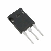
TO-247AC
Max.
600 52 30 104 104 10 ±20 170 200 78 -55 to +150 300 (0.063 in. (1.6mm) from case) 10 lbfin (1.1Nm)
Units
V A
µs V mJ W
°C
Thermal Resistance
Parameter
RθJC RθCS RθJA Wt Junction-to-Case Case-to-Sink, Flat, Greased Surface Junction-to-Ambient, typical socket mount Weight
Typ.
0.24 6 (0.21)
Max.
0.64 40
Units
°C/W g (oz)
www.irf.com
7/26/04
1
�IRG4PC50KPbF
Electrical Characteristics @ TJ = 25°C (unless otherwise specified)
Parameter Min. Typ. Collector-to-Emitter Breakdown Voltage 600 Emitter-to-Collector Breakdown Voltage 18 ∆V(BR)CES/∆TJ Temperature Coeff. of Breakdown Voltage 0.47 1.84 Collector-to-Emitter Saturation Voltage 2.19 VCE(ON) 1.79 VGE(th) Gate Threshold Voltage 3.0 ∆VGE(th)/∆TJ Temperature Coeff. of Threshold Voltage -12 gfe Forward Transconductance
17 24 ICES Zero Gate Voltage Collector Current IGES Gate-to-Emitter Leakage Current V(BR)CES V(BR)ECS Max. Units Conditions V VGE = 0V, IC = 250µA V VGE = 0V, IC = 1.0A V/°C VGE = 0V, IC = 1.0mA 2.2 IC = 30A VGE = 15V IC = 52A See Fig.2, 5 V IC = 30A , TJ = 150°C 6.0 VCE = VGE, IC = 250µA mV/°C VCE = VGE, IC = 250µA S VCE = 100 V, IC = 30A 250 VGE = 0V, VCE = 600V µA 2.0 VGE = 0V, VCE = 10V, TJ = 25°C 5000 VGE = 0V, VCE = 600V, TJ = 150°C ±100 n A VGE = ±20V
Switching Characteristics @ TJ = 25°C (unless otherwise specified)
Qg Qge Qgc td(on) tr td(off) tf Eon Eoff Ets tsc td(on) tr td(off) tf Ets LE Cies Coes Cres Notes: Parameter Total Gate Charge (turn-on) Gate - Emitter Charge (turn-on) Gate - Collector Charge (turn-on) Turn-On Delay Time Rise Time Turn-Off Delay Time Fall Time Turn-On Switching Loss Turn-Off Switching Loss Total Switching Loss Short Circuit Withstand Time Turn-On Delay Time Rise Time Turn-Off Delay Time Fall Time Total Switching Loss Internal Emitter Inductance Input Capacitance Output Capacitance Reverse Transfer Capacitance Min. 10 Typ. 200 25 85 38 34 160 79 0.49 0.68 1.12 37 35 260 170 2.34 13 3200 370 95 Max. Units Conditions 300 IC = 30A 38 nC VCC = 400V See Fig.8 130 VGE = 15V TJ = 25°C ns 240 IC = 30A, VCC = 480V 120 VGE = 15V, RG = 5.0Ω Energy losses include "tail" mJ See Fig. 9,10,14 1.4 µs VCC = 400V, TJ = 125°C VGE = 15V, RG = 10Ω , VCPK < 500V TJ = 150°C, IC = 30A, VCC = 480V ns VGE = 15V, RG = 5.0Ω Energy losses include "tail" mJ See Fig. 11,14 nH Measured 5mm from package VGE = 0V pF VCC = 30V See Fig. 7 = 1.0MHz
Repetitive rating; VGE = 20V, pulse width limited by
max. junction temperature. ( See fig. 13b )
Repetitive rating; pulse width limited by maximum
junction temperature.
VCC = 80%(VCES), VGE = 20V, L = 10µH, RG = 5.0 Ω
Pulse width ≤ 80µs; duty factor ≤ 0.1%.
Pulse width 5.0µs, single shot.
2
www.irf.com
�IRG4PC50KPbF
70 For both: 60
Triangular wave:
50
Duty cycle: 50% TJ = 125°C Tsink = 90°C Gate drive as specified Power Dissipation = 40W
Clamp voltage: 80% of rated
40
Square wave: 60% of rated voltage
I
30
20
10
Ideal diodes
0 0.1 1 10
A
100
f, Frequency (kHz)
Fig. 1 - Typical Load Current vs. Frequency
(Load Current = IRMS of fundamental)
1000
1000
I C , Collector-to-Emitter Current (A)
100
TJ = 25 °C TJ = 150 °C
I C , Collector-to-Emitter Current (A)
100
TJ = 150 °C
10
10
TJ = 25 °C V CC = 50V 5µs PULSE WIDTH
5 6 7 8 9 10 11 12
1
V GE = 15V 20µs PULSE WIDTH
1 10
1
VCE , Collector-to-Emitter Voltage (V)
VGE , Gate-to-Emitter Voltage (V)
Fig. 2 - Typical Output Characteristics
Fig. 3 - Typical Transfer Characteristics
www.irf.com
3
�IRG4PC50KPbF
60
3.0
50
VCE , Collector-to-Emitter Voltage(V)
VGE = 15V 80 us PULSE WIDTH IC = 60 A
Maximum DC Collector Current(A)
40
30
2.0
IC = 30 A
20
IC = 15 A
10
0 25 50 75 100 125 150
1.0 -60 -40 -20
0
20
40
60
80 100 120 140 160
TC , Case Temperature ( ° C)
TJ , Junction Temperature ( °C)
Fig. 4 - Maximum Collector Current vs. Case Temperature
Fig. 5 - Typical Collector-to-Emitter Voltage vs. Junction Temperature
1
Thermal Response (Z thJC )
0.50 0.20 0.1 0.10 0.05 0.02 0.01 SINGLE PULSE (THERMAL RESPONSE) PDM t1 t2 Notes: 1. Duty factor D = t 1 / t 2 2. Peak TJ = PDM x Z thJC + TC 0.0001 0.001 0.01 0.1 1
0.01
0.001 0.00001
t1 , Rectangular Pulse Duration (sec)
Fig. 6 - Maximum Effective Transient Thermal Impedance, Junction-to-Case
4
www.irf.com
�IRG4PC50KPbF
5000
4000
VGE , Gate-to-Emitter Voltage (V)
VGE = 0V, f = 1MHz Cies = Cge + Cgc , Cce SHORTED Cres = Cgc Coes = Cce + Cgc
20
VCC = 400V I C = 30A
16
C, Capacitance (pF)
Cies
3000
12
2000
8
1000
4
0 1 10
Coes Cres
100
0 0 40 80 120 160 200
VCE , Collector-to-Emitter Voltage (V)
QG , Total Gate Charge (nC)
Fig. 7 - Typical Capacitance vs. Collector-to-Emitter Voltage
Fig. 8 - Typical Gate Charge vs. Gate-to-Emitter Voltage
4.0
Total Switching Losses (mJ)
3.0
Total Switching Losses (mJ)
V CC = 480V V GE = 15V TJ = 25 ° C I C = 30A
100
RG = 5.0Ω Ohm VGE = 15V VCC = 480V
10
IC = 60 A IC = 30 A
2.0
1
IC = 15 A
1.0
0.0 0
Ω RG , Gate Resistance (Ohm) (Ω)
10
20
30
40
50
0.1 -60 -40 -20
0
20
40
60
80 100 120 140 160
TJ , Junction Temperature ( °C )
Fig. 9 - Typical Switching Losses vs. Gate Resistance
Fig. 10 - Typical Switching Losses vs. Junction Temperature
www.irf.com
5
�IRG4PC50KPbF
8.0
6.0
I C, Collector-to-Emitter Current (A)
Total Switching Losses (mJ)
RG TJ VCC VGE
5.0Ω = 5.0Ohm = 150 °C = 480V = 15V
1000
VGE = 20V T J = 125 oC
4.0
100
2.0
SAFE OPERATING AREA
0.0 10 20 30 40 50 60
10 1 10 100 1000
I C , Collector-to-emitter Current (A)
VCE , Collector-to-Emitter Voltage (V)
Fig. 11 - Typical Switching Losses vs. Collector-to-Emitter Current
Fig. 12 - Turn-Off SOA
6
www.irf.com
�IRG4PC50KPbF
L 50V 1000V VC *
D.U.T.
RL = 0 - 480V
480V 4 X IC@ 25°C
c
480µF 960V
d
* Driver same type as D.U.T.; Vc = 80% of Vce(max) * Note: Due to the 50V power supply, pulse width and inductor will increase to obtain rated Id.
Fig. 13a - Clamped Inductive
Load Test Circuit
Fig. 13b - Pulsed Collector
Current Test Circuit
IC L Driver* 50V D.U.T. VC
Fig. 14a - Switching Loss
Test Circuit
* Driver same type as D.U.T., VC = 480V
Ã
1000V
d
e
c d
90%
e
VC 90%
10%
t d(off)
Fig. 14b - Switching Loss
Waveforms
10% I C 5% t d(on)
tr E on E ts = (Eon +Eoff )
tf t=5µs E off
www.irf.com
7
�IRG4PC50KPbF
TO-247AC Package Outline
Dimensions are shown in millimeters (inches)
TO-247AC Part Marking Information
EXAMPLE: THIS IS AN IRFPE30 WIT H ASS EMBLY LOT CODE 5657 ASS EMBLED ON WW 35, 2000 IN THE ASS EMBLY LINE "H"
Note: "P" in assembly line position indicates "Lead-Free"
PART NUMBER INT ERNATIONAL RECT IFIER LOGO AS S EMBLY LOT CODE
IRFPE30
56 035H 57
DATE CODE YEAR 0 = 2000 WEEK 35 LINE H
Data and specifications subject to change without notice.
IR WORLD HEADQUARTERS: 233 Kansas St., El Segundo, California 90245, USA Tel: (310) 252-7105 TAC Fax: (310) 252-7903 Visit us at www.irf.com for sales contact information. 07/04
8
www.irf.com
�