PD -95186
IRG4PC50UPbF
INSULATED GATE BIPOLAR TRANSISTOR
Features
• UltraFast: Optimized for high operating frequencies 8-40 kHz in hard switching, >200 kHz in resonant mode • Generation 4 IGBT design provides tighter parameter distribution and higher efficiency than Generation 3 • Industry standard TO-247AC package • Lead-Free
C
UltraFast Speed IGBT
VCES = 600V
G E
VCE(on) typ. = 1.65V
@VGE = 15V, IC = 27A
n-channel
Benefits
• Generation 4 IGBT's offer highest efficiency available • IGBT's optimized for specified application conditions • Designed to be a "drop-in" replacement for equivalent industry-standard Generation 3 IR IGBT's
Absolute Maximum Ratings
Parameter
VCES IC @ TC = 25°C IC @ TC = 100°C ICM ILM VGE EARV PD @ TC = 25°C PD @ TC = 100°C TJ TSTG Collector-to-Emitter Breakdown Voltage Continuous Collector Current Continuous Collector Current Pulsed Collector Current Q Clamped Inductive Load Current R Gate-to-Emitter Voltage Reverse Voltage Avalanche Energy S Maximum Power Dissipation Maximum Power Dissipation Operating Junction and Storage Temperature Range Soldering Temperature, for 10 seconds Mounting torque, 6-32 or M3 screw.
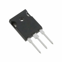
TO-247AC
Max.
600 55 27 220 220 ± 20 20 200 78 -55 to + 150 300 (0.063 in. (1.6mm from case ) 10 lbf•in (1.1N•m)
Units
V A
V mJ W
°C
Thermal Resistance
Parameter
RθJC RθCS RθJA Wt Junction-to-Case Case-to-Sink, Flat, Greased Surface Junction-to-Ambient, typical socket mount Weight
Typ.
---0.24 ---6 (0.21)
Max.
0.64 ---40 ----
Units
°C/W g (oz)
www.irf.com
1
04/26/04
�IRG4PC50UPbF
Electrical Characteristics @ TJ = 25°C (unless otherwise specified)
Parameter Min. Typ. Collector-to-Emitter Breakdown Voltage 600 ---Emitter-to-Collector Breakdown Voltage T 18 ---∆V(BR)CES/∆TJ Temperature Coeff. of Breakdown Voltage ---- 0.60 ---- 1.65 VCE(ON) Collector-to-Emitter Saturation Voltage ---- 2.0 ---- 1.6 VGE(th) Gate Threshold Voltage 3.0 ---∆VGE(th)/∆TJ Temperature Coeff. of Threshold Voltage ---- -13 gfe Forward Transconductance U 16 24 ---- ---ICES Zero Gate Voltage Collector Current ---- ------- ---IGES Gate-to-Emitter Leakage Current ---- ---V(BR)CES V(BR)ECS Max. Units Conditions ---V VGE = 0V, IC = 250µA ---V VGE = 0V, IC = 1.0A ---- V/°C VGE = 0V, IC = 1.0mA 2.0 IC = 27A VGE = 15V ---IC = 55A See Fig.2, 5 V ---IC = 27A , TJ = 150°C 6.0 VCE = VGE, IC = 250µA ---- mV/°C VCE = VGE, IC = 250µA ---S VCE ≥ 15V, IC = 27A 250 µA VGE = 0V, VCE = 600V 2.0 VGE = 0V, VCE = 10V, TJ = 25°C 5000 VGE = 0V, VCE = 600V, TJ = 150°C ±100 nA VGE = ±20V
Switching Characteristics @ TJ = 25°C (unless otherwise specified)
Qg Qge Qgc td(on) tr td(off) tf Eon Eoff Ets td(on) tr td(off) tf Ets LE Cies Coes Cres Notes: Parameter Total Gate Charge (turn-on) Gate - Emitter Charge (turn-on) Gate - Collector Charge (turn-on) Turn-On Delay Time Rise Time Turn-Off Delay Time Fall Time Turn-On Switching Loss Turn-Off Switching Loss Total Switching Loss Turn-On Delay Time Rise Time Turn-Off Delay Time Fall Time Total Switching Loss Internal Emitter Inductance Input Capacitance Output Capacitance Reverse Transfer Capacitance Min. ---------------------------------------------------------Typ. 180 25 61 32 20 170 88 0.12 0.54 0.66 31 23 230 120 1.6 13 4000 250 52 Max. Units Conditions 270 IC = 27A 38 nC VCC = 400V See Fig. 8 90 VGE = 15V ------TJ = 25°C ns 260 IC = 27A, VCC = 480V 130 VGE = 15V, RG = 5.0Ω ---Energy losses include "tail" ---mJ See Fig. 10, 11, 13, 14 0.9 ---TJ = 150°C, ---IC = 27A, VCC = 480V ns ---VGE = 15V, RG = 5.0Ω ---Energy losses include "tail" ---mJ See Fig. 13, 14 ---nH Measured 5mm from package ---VGE = 0V ---pF VCC = 30V See Fig. 7 ---ƒ = 1.0MHz
Q Repetitive rating; VGE = 20V, pulse width limited by
max. junction temperature. ( See fig. 13b )
R VCC = 80%(VCES), VGE = 20V, L = 10µH, RG = 5.0Ω,
(See fig. 13a)
T Pulse width ≤ 80µs; duty factor ≤ 0.1%. U Pulse width 5.0µs, single shot.
S Repetitive rating; pulse width limited by maximum
junction temperature.
2
www.irf.com
�IRG4PC50UPbF
80
F o r b o th :
T rian gu la r w a ve:
60
L oad C urre nt (A )
D u t y c yc le: 5 0% T J = 1 2 5 °C T s in k = 9 0 °C G a te d r ive a s sp ec ified P o w e r D is sip atio n = 40 W
C la m p vo lta g e : 8 0 % o f ra te d
S q u are w a ve :
40
6 0 % o f ra ted vo ltag e
20
Idea l d io des
0 0.1 1 10
A
100
f, F re q u e nc y ( k H z )
Fig. 1 - Typical Load Current vs. Frequency
(For square wave, I=IRMS of fundamental; for triangular wave, I=IPK)
I C , C o lle ctor-to-E m itter Cu rre n t (A )
1000
1000
100
I C , C ollec to r-to-Em itte r C u rre nt (A)
100
10
T J = 1 5 0 °C
TJ = 1 5 0°C
T J = 2 5 °C
1
10
T J = 2 5 °C
0.1 0 1
VGE = 15V 2 0 µ s P U L S E W ID T H
A
10
1 4 6 8
V C C = 10 V 5 µs P U L S E W IDTH A
10 12
VC E , C o lle c to r-to -E m itte r V o lta g e ( V )
VG E , G a te -to -E m itte r V o lta g e ( V )
Fig. 2 - Typical Output Characteristics www.irf.com
Fig. 3 - Typical Transfer Characteristics 3
�IRG4PC50UPbF
60
50
V CE , C olle ctor-to-E m itte r V oltage (V)
V G E = 15 V
2.5
M aximum D C Collector Current (A )
V G E = 1 5V 8 0 µs P U L S E W ID TH IC = 5 4 A
40
2.0
30
IC = 2 7 A
1.5
20
IC = 14 A
10
0 25 50 75 100 125 150
1.0 -60 -40 -20 0 20 40 60 80 100 120
A
140 160
T C , C ase Tem perature (°C)
T J , Ju n c tio n Te m p e ra tu re ( °C )
Fig. 4 - Maximum Collector Current vs. Case Temperature
Fig. 5 - Collector-to-Emitter Voltage vs. Junction Temperature
1
T h e rm a l R e s p o n se (Z thJ C )
D = 0 .5 0
0 .2 0
0 .1
0 .1 0 0 .0 5 0 .0 2 0 .0 1 S IN G L E P U L S E (T H E R M A L R E S P O N S E )
N ote s : 1 . D u ty f ac t or D = t 1 /t 2 PD M
t
1 t 2
0 .0 1 0 .0 0 0 0 1
2 . P e a k TJ = P D M x Z th J C + T C
0 .0 0 0 1
0 .0 0 1
0 .0 1
0 .1
1
10
t 1 , R e c ta n g u la r P u ls e D ura tio n (s e c )
Fig. 6 - Maximum Effective Transient Thermal Impedance, Junction-to-Case 4 www.irf.com
�IRG4PC50UPbF
8000
V G E , Gate-to-Emitter Voltage (V)
V GE C ie s C re s C o es
= = = =
0V , f = 1M Hz C ge + C gc , C ce SH OR T ED C gc C ce + C gc
20
VC E = 4 00V I C = 27A
C, Capacitance (pF)
16
6000
C ie s
12
4000
C oe s
2000
8
C r es
4
0 1 10
A
100
0 0 40 80 120 160
A
200
VC E , C o lle c to r-to -E m itte r V o lta g e ( V )
Q g , Total Gate Char g e ( nC )
Fig. 7 - Typical Capacitance vs. Collector-to-Emitter Voltage
Fig. 8 - Typical Gate Charge vs. Gate-to-Emitter Voltage
2.2 2.0
To ta l S w itc h in g L os se s (m J)
VC C VG E TJ IC
= 4 80V = 15V = 25°C = 27A
10
R G = 5 .0 Ω V GE = 15V V CC = 480V
IC = 5 4 A
Total Switching Losses (mJ)
1.8 1.6 1.4 1.2 1.0 0.8 0.6 0 10 20 30 40 50
IC = 2 7A
1
IC = 1 4 A
A
60
0.1 -60 -40 -20 0 20 40 60 80 100 120 140
A
160
R G , Gate Resistance ( Ω)
TJ , J u n ctio n T e m p e ra tu re ( °C )
Fig. 9 - Typical Switching Losses vs. Gate Resistance www.irf.com
Fig. 10 - Typical Switching Losses vs. Junction Temperature 5
�IRG4PC50UPbF
3.0
Total Switc hing Losses (mJ )
I C , C ollector-to-E m itter Current (A )
RG TJ V CC V GE
= 5 .0 Ω = 1 5 0 °C = 480V = 15V
1000
VG E E 2 0V G= T J = 125 °C
2.0
100
S A FE O P E R A T IN G A R E A
1.0
10
0.0 0 10 20 30 40 50
A
1 1 10 100 1000
I C , C o lle cto r-to -E m itte r C u rre n t ( A )
V C E , Collecto r-to-E m itter V oltage (V )
Fig. 11 - Typical Switching Losses vs. Collector-to-Emitter Current
Fig. 12 - Turn-Off SOA
6
www.irf.com
�IRG4PC50UPbF
L 50V 1 00 0V VC *
D .U .T.
RL = 0 - 480V
480V 4 X IC@25°C
480µF 960V
Q
R
* Driver s am e ty p e as D .U .T.; Vc = 80% of V ce ( m ax ) * Note: D ue to the 50V p ow er s u p p l y , p ulse w idth a nd inductor w ill inc rea se to obta in ra ted Id.
Fig. 13a - Clamped Inductive
Load Test Circuit
Fig. 13b - Pulsed Collector
Current Test Circuit
IC L D river* 50V 1000V Q� R S VC D .U .T.
Fig. 14a - Switching Loss
Test Circuit
* Driver same type as D.U.T., VC = 480V
Q
R
9 0%
S
1 0% 90 %
VC
t d (o ff)
Fig. 14b - Switching Loss
Waveforms
10 % IC 5% t d (o n )
tr E on E ts = ( Eo n +E o ff )
tf t =5µ s E o ff
www.irf.com
7
�IRG4PC50UPbF
TO-247AC Package Outline
Dimensions are shown in millimeters (inches)
TO-247AC Part Marking Information
E XAMPL E : T HIS IS AN IR F PE 30 WIT H AS S E MB LY L OT CODE 5657 AS S E MB L E D ON WW 35, 2000 IN T H E AS S E MB LY L INE "H"
Note: "P" in assembly line position indicates "Lead-Free"
INT E R NAT IONAL R E CT IF IE R L OGO AS S E MB L Y L OT CODE
PAR T NU MB E R
IR F PE 30
56 035H 57
DAT E CODE YE AR 0 = 2000 WE E K 35 L INE H
IR WORLD HEADQUARTERS: 233 Kansas St., El Segundo, California 90245, USA Tel: (310) 252-7105 TAC Fax: (310) 252-7903 Visit us at www.irf.com for sales contact information. Data and specifications subject to change without notice. 04/04
8
www.irf.com
�Note: For the most current drawings please refer to the IR website at: http://www.irf.com/package/
�