PD 91736A
IRG4RC10KD
INSULATED GATE BIPOLAR TRANSISTOR WITH ULTRAFAST SOFT RECOVERY DIODE
Features
• Short Circuit Rated UltraFast: Optimized for high operating frequencies >5.0 kHz , and Short Circuit Rated to 10µs @ 125°C, VGE = 15V • Generation 4 IGBT design provides tighter parameter distribution and higher efficiency than previous generation • IGBT co-packaged with HEXFREDTM ultrafast, ultra-soft-recovery anti-parallel diodes for use in bridge configurations • Industry standard TO-252AA package
C
Short Circuit Rated UltraFast IGBT
VCES = 600V
G E
VCE(on) typ. = 2.39V
@VGE = 15V, IC = 5.0A
n-ch an nel
Benefits
• Latest generation 4 IGBT's offer highest power density motor controls possible • HEXFREDTM diodes optimized for performance with IGBTs. Minimized recovery characteristics reduce noise, EMI and switching losses • For hints see design tip 97003
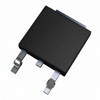
D-PAK TO-252AA
Absolute Maximum Ratings
Parameter
VCES IC @ TC = 25°C IC @ TC = 100°C ICM ILM IF @ TC = 100°C IFM tsc VGE PD @ TC = 25°C PD @ TC = 100°C TJ TSTG Collector-to-Emitter Voltage Continuous Collector Current Continuous Collector Current Pulsed Collector Current�Q Clamped Inductive Load Current R Diode Continuous Forward Current Diode Maximum Forward Current Short Circuit Withstand Time Gate-to-Emitter Voltage Maximum Power Dissipation Maximum Power Dissipation Operating Junction and Storage Temperature Range Soldering Temperature, for 10 sec.
Max.
600 9.0 5.0 18 18 4.0 16 10 ± 20 38 15 -55 to +150 300 (0.063 in. (1.6mm) from case)
Units
V
A
µs V W
°C
Thermal Resistance
Parameter
RθJC RθJC RθJA Wt Junction-to-Case - IGBT Junction-to-Case - Diode Junction-to-Ambient (PCB mount)* Weight
Typ.
––– ––– ––– 0.3 (0.01)
Max.
3.3 7.0 50 –––
Units
°C/W g (oz)
* When mounted on 1" square PCB (FR-4 or G-10 Material). For recommended footprint and soldering techniques refer to application note #AN-994
www.irf.com
1
12/30/00
�IRG4RC10KD
Electrical Characteristics @ TJ = 25°C (unless otherwise specified)
V(BR)CES
∆V(BR)CES/∆TJ
VCE(on)
VGE(th) ∆VGE(th)/∆TJ gfe ICES VFM IGES
Parameter Min. Typ. Max. Units Conditions Collector-to-Emitter Breakdown Voltageƒ 600 — — V VGE = 0V, IC = 250µA Temperature Coeff. of Breakdown Voltage — 0.58 — V/°C VGE = 0V, IC = 1.0mA Collector-to-Emitter Saturation Voltage — 2.39 2.62 IC = 5.0A VGE = 15V See Fig. 2, 5 — 3.25 — V IC = 9.0A — 2.63 — IC = 5.0A, TJ = 150°C Gate Threshold Voltage 3.0 — 6.5 VCE = VGE, IC = 250µA Temperature Coeff. of Threshold Voltage — -11 — mV/°C VCE = VGE, IC = 250µA Forward Transconductance „ 1.2 1.8 — S VCE = 50V, IC = 5.0A Zero Gate Voltage Collector Current — — 250 µA VGE = 0V, VCE = 600V — — 1000 VGE = 0V, VCE = 600V, TJ = 150°C Diode Forward Voltage Drop — 1.5 1.8 V IC = 4.0A See Fig. 13 — 1.4 1.7 IC = 4.0A, TJ = 150°C Gate-to-Emitter Leakage Current — — ±100 nA VGE = ±20V
Switching Characteristics @ TJ = 25°C (unless otherwise specified)
Qg Qge Qgc td(on) tr td(off) tf Eon Eoff Ets tsc td(on) tr td(off) tf Ets LE Cies Coes Cres trr Irr Qrr di(rec)M /dt Parameter Total Gate Charge (turn-on) Gate - Emitter Charge (turn-on) Gate - Collector Charge (turn-on) Turn-On Delay Time Rise Time Turn-Off Delay Time Fall Time Turn-On Switching Loss Turn-Off Switching Loss Total Switching Loss Short Circuit Withstand Time Turn-On Delay Time Rise Time Turn-Off Delay Time Fall Time Total Switching Loss Internal Emitter Inductance Input Capacitance Output Capacitance Reverse Transfer Capacitance Diode Reverse Recovery Time Diode Peak Reverse Recovery Current Diode Reverse Recovery Charge Diode Peak Rate of Fall of Recovery During tb Min. — — — — — — — — — — 10 — — — — — — — — — — — — — — — — — Typ. 19 2.9 9.8 49 28 97 140 0.25 0.14 0.39 — 46 32 100 310 0.56 7.5 220 29 7.5 28 38 2.9 3.7 40 70 280 235 Max. Units Conditions 29 IC = 5.0A 4.3 nC VCC = 400V See Fig.8 15 VGE = 15V — — TJ = 25°C ns 150 IC = 5.0A, VCC = 480V 210 VGE = 15V, RG = 100Ω — Energy losses include "tail" — mJ and diode reverse recovery 0.48 See Fig. 9,10,14 — µs VCC = 360V, TJ = 125°C VGE = 15V, RG = 100Ω , VCPK < 500V — TJ = 150°C, See Fig. 10,11,14 — IC = 5.0A, VCC = 480V ns — VGE = 15V, RG = 100Ω — Energy losses include "tail" — mJ and diode reverse recovery — nH Measured 5mm from package — VGE = 0V — pF VCC = 30V See Fig. 7 — ƒ = 1.0MHz 42 ns TJ = 25°C See Fig. 57 TJ = 125°C 14 IF = 4.0A 5.2 A TJ = 25°C See Fig. 6.7 TJ = 125°C 15 VR = 200V 60 nC TJ = 25°C See Fig. 105 TJ = 125°C 16 di/dt = 200A/µs — A/µs TJ = 25°C See Fig. — TJ = 125°C 17
2
www.irf.com
�IRG4RC10KD
1.6
For both:
LOAD CURRENT (A)
1.2
D uty cy cle: 50% TJ = 125 ° C T s ink = 55 ° C 90 G ate drive as specified
P ow e r Dis sip ation = 1.4 W S q u a re w a v e :
0.8
6 0% of rate d volta ge
I
0.4
Id e a l d io d e s
0.0 0.1 1 10 100
f, Frequency (KHz)
Fig. 1 - Typical Load Current vs. Frequency
(Load Current = IRMS of fundamental)
100
100
TJ = 25 °C �
10
I C , Collector-to-Emitter Current (A)
I C , Collector Current (A)
T = 150 °C � J
10
TJ = 150 °C � TJ = 25 °C �
1 5 10
1 1.0
�
V GE = 15V 20µs PULSE WIDTH
5.0 6.0 2.0 3.0 4.0 7.0
V = 50V � 5µs PULSE WIDTH
CC 15 20
VCE , Collector-to-Emitter Voltage (V)
VGE , Gate-to-Emitter Voltage (V)
Fig. 2 - Typical Output Characteristics
Fig. 3 - Typical Transfer Characteristics
www.irf.com
3
�IRG4RC10KD
10 5.0
8
VCE , Collector-to-Emitter Voltage(V)
V = 15V � 80 us PULSE WIDTH
GE
� I C = 10 A
Maximum DC Collector Current(A)
4.0
6
3.0
� IC = 5 A � I C = 2.5 A
4
2.0
2
0 25 50 75 100 125 150
1.0 -60 -40 -20
0
20
40
60
80 100 120 140 160
TC , Case Temperature ( °C)
TJ , Junction Temperature ( ° C)
Fig. 4 - Maximum Collector Current vs. Case Temperature
Fig. 5 - Typical Collector-to-Emitter Voltage vs. Junction Temperature
10
Thermal Response (Z thJC )
D = 0.50 1 0.20 0.10 0.05 0.02 0.01
0.1
�
SINGLE PULSE (THERMAL RESPONSE)
0.01 0.00001
�
Notes: 1. Duty factor D = t 1 / t 2 2. Peak TJ = PDM x Z thJC + TC 0.1 0.0001 0.001 0.01
�
P DM t1 t2 1
t1 , Rectangular Pulse Duration (sec)
Fig. 6 - Maximum Effective Transient Thermal Impedance, Junction-to-Case
4
www.irf.com
�IRG4RC10KD
400
VGE , Gate-to-Emitter Voltage (V)
300
�
VGE = 0V, f = 1MHz Cies = Cge + Cgc , Cce SHORTED Cres = Cgc Coes = Cce + Cgc
20
�
VCC = 400V I C = 5.0A
16
C, Capacitance (pF)
Cies �
200
12
8
100
C� oes C� res
4
0 1 10 100
0 0 4 8 12 16 20
VCE , Collector-to-Emitter Voltage (V)
QG , Total Gate Charge (nC)
Fig. 7 - Typical Capacitance vs. Collector-to-Emitter Voltage
0.40
Fig. 8 - Typical Gate Charge vs. Gate-to-Emitter Voltage
10
Total Switching Losses (mJ)
Total Switching Losses (mJ)
V CC = 480V V GE = 15V TJ = 25 ° C 0.38 I C = 5.0A
�
�
50 Ω RG = Ohm VGE = 15V VCC = 480V
0.36
� IC = 10 A
1
0.34
� IC = 5 A � IC = 2.5 A
0.32
0.30 0 20 40 60 80 100
0.1 -60 -40 -20
0
20
40
60
80 100 120 140 160
RG , Gate Resistance
(Ω)
TJ , Junction Temperature ( °C )
Fig. 9 - Typical Switching Losses vs. Gate Resistance
Fig. 10 - Typical Switching Losses vs. Junction Temperature
www.irf.com
5
�IRG4RC10KD
2.0
1.5
1.0
I C, Collector-to-Emitter Current (A)
4 6 8 10
Total Switching Losses (mJ)
�
RG TJ VCC VGE
= 50 Ω Ohm = 150° C = 480V = 15V
100
�
VGE = 20V T J = 125 o C
10
0.5
0.0 0 2
�SAFE OPERATING AREA
1 1 10 100 1000
I C , Collector Current (A)
VCE, Collector-to-Emitter Voltage (V)
Fig. 11 - Typical Switching Losses vs. Collector-to-Emitter Current
100
Fig. 12 - Turn-Off SOA
10
TJ = 150 ° C TJ = 125 ° C T = 25 ° C
J
1
0.1 0.0 1.0 2.0 3.0 4.0 5.0 6.0
F orward V olta g e D rop - V F M V ) (
Fig. 13 - Maximum Forward Voltage Drop vs. Instantaneous Forward Current
6
www.irf.com
�IRG4RC10KD
50 14 VR = 20 0V T J = 1 25 ° C T J = 2 5 °C 45
I F = 8.0A I F = 4.0A
12
I F = 8.0A
10
40
I F = 4.0A
trr- (nC)
Irr- ( A)
8
35
6 30 4
25 VR = 2 00 V TJ = 1 2 5°C T J = 2 5 °C 20 100 1000 2
di f /dt - ( A/ µ s )
0 100
1000
di f /dt - ( A/ µ s )
Fig. 14 - Typical Reverse Recovery vs. dif/dt
200 VR = 2 00 V T J = 1 25 ° C T J = 2 5 °C 160
Fig. 15 - Typical Recovery Current vs. dif/dt
1000 VR = 20 0V T J = 1 25 ° C T J = 2 5 °C
I F = 8.0A
I F = 8.0A
di (rec) M/dt- (A /µs)
120
I F = 4.0A
I F = 4.0A
Qrr- (nC)
80 40
0 100
di f /dt - ( A/ µ s )
1000
100 100
A 1000
di f /dt - ( A/ µ s )
Fig. 16 - Typical Stored Charge vs. dif/dt
Fig. 17 - Typical di(rec)M/dt vs. dif/dt,
www.irf.com
7
�IRG4RC10KD
Same ty pe device as D .U.T.
80% of Vce
430µF D .U .T.
Vge VC 90% 10% 90%
td(off)
Fig. 18a - Test Circuit for Measurement of
ILM, Eon, Eoff(diode), trr, Qrr, Irr, td(on), tr, td(off), tf
10% IC 5% t d(on)
tr Eon E ts = (Eon +Eoff )
tf t=5µs Eoff
Fig. 18b - Test Waveforms for Circuit of Fig. 18a, Defining
Eoff, td(off), tf
G A T E V O L T A G E D .U .T . 1 0 % +V g +Vg
trr Ic
Q rr =
∫
trr id ddt Ic t tx
tx 10% Vcc Vce Vcc 1 0 % Ic 9 0 % Ic D UT VO LTAG E AN D CU RRE NT Ip k Ic
1 0 % Irr V cc
V pk Irr
D IO D E R E C O V E R Y W A V E FO R M S td (o n ) tr 5% Vce t2 Vce d E o n = V ce ieIc t dt t1 t2 D IO D E R E V E R S E REC OVERY ENER GY t3 t4
∫
E re c =
∫
t4 V d idIc t dt Vd d t3
t1
Fig. 18c - Test Waveforms for Circuit of Fig. 18a,
Defining Eon, td(on), tr
Fig. 18d - Test Waveforms for Circuit of Fig. 18a,
Defining Erec, trr, Qrr, Irr
8
www.irf.com
�IRG4RC10KD
V g G AT E SIG NA L DE VIC E U ND E R T E S T CU R RE NT D .U .T.
VO L TA G E IN D.U .T.
CU R RE NT IN D 1
t0
t1
t2
Figure 18e. Macro Waveforms for Figure 18a's Test Circuit
L 1000V 50V 6000µ F 100 V Vc* D.U.T.
RL= 0 - 480V
480V 4 X IC @25°C
Figure 19. Clamped Inductive Load Test Circuit
Figure 20. Pulsed Collector Current Test Circuit
Package Outline
TO-252AA Outline Dimensions are shown in millimeters (inches)
6.7 3 ( .2 65 ) 6.3 5 ( .2 50 ) -A5 .46 ( .21 5 ) 5 .21 ( .20 5 ) 4 6.45 ( .24 5 ) 5.68 ( .22 4 ) 6.2 2 ( .2 45 ) 5.9 7 ( .2 35 ) 1 .0 2 (.04 0 ) 1 .6 4 (.02 5 ) 1 2 3 0.51 ( .0 2 0 ) M IN . 10 .42 ( .41 0 ) 9 .4 0 ( .3 70 ) 1 .2 7 ( .0 50 ) 0 .8 8 ( .0 35 ) 2.3 8 ( .0 94 ) 2.1 9 ( .0 86 ) 1.1 4 ( .0 45 ) 0.8 9 ( .0 35 ) 0.58 ( .02 3 ) 0.46 ( .01 8 )
L E A D A S S IG N M E NT S 1 - G A TE 2 - D R A IN 3 - SOURCE 4 - D R A IN
LEAD ASSIGNMENTS 1 - GATE 2 - COLLECTOR
-B 1 .5 2 ( .06 0 ) 1 .1 5 ( .04 5 ) 3X 1.1 4 ( .0 45 ) 2 X 0.7 6 ( .0 30 ) 2.28 ( .0 90 ) 4.57 ( .18 0 ) 0.89 ( .0 35 ) 0.64 ( .0 25 ) 0 .2 5 ( .0 10 ) M AMB
0 .5 8 ( .0 23 ) 0 .4 6 ( .0 18 )
3 - EMITTER 4 - COLLECTOR
N OT E S: 1 D IM EN SIO N IN G & TO L E R AN C IN G PE R A N SI Y 14 .5 M, 19 82. 2 C O N TR O LL ING D IM E N S IO N : IN C H. 3 C O N FO R M S T O JE D E C O U TL IN E TO - 252 A A. 4 D IM EN SIO N S S H OW N A RE B E F O RE S O LD E R D IP , S O L D ER D IP M A X. + 0.16 ( .0 06 ) .
www.irf.com
9
�IRG4RC10KD
Notes:
Q Repetitive rating: VGE=20V; pulse width limited by maximum junction temperature (figure 20) R VCC=80%(VCES), VGE=20V, L=10µH, RG= 100Ω (figure 19) S Pulse width ≤ 80µs; duty factor ≤ 0.1%. T Pulse width 5.0µs, single shot.
Tape & Reel Information
TO-252AA
TR TRR TR L
1 6 .3 ( .6 4 1 ) 1 5 .7 ( .6 1 9 )
16 .3 ( .64 1 ) 15 .7 ( .61 9 )
12 .1 ( .4 7 6 ) 11 .9 ( .4 6 9 )
F E E D D IR E C T IO N
8 .1 ( .3 18 ) 7 .9 ( .3 12 )
FE E D D IR E C T IO N
NOTES : 1 . C O N T R O L L IN G D IM EN S IO N : M IL L IM E T E R . 2 . A L L D IM EN S IO N S A R E S H O W N IN M IL L IM E T E R S ( IN C H E S ). 3 . O U T L IN E C O N F O R M S T O E IA -4 8 1 & E IA -5 4 1 .
1 3 IN C H
16 m m NOTES : 1 . O U T L IN E C O N F O R M S T O E IA -4 8 1 .
IR WORLD HEADQUARTERS: 233 Kansas St., El Segundo, California 90245, USA Tel: (310) 252-7105 TAC Fax: (310) 252-7903 Visit us at www.irf.com for sales contact information. Data and specifications subject to change without notice. 12/00
10
www.irf.com
�