PD - 96305
INSULATED GATE BIPOLAR TRANSISTOR Features
• • • • • • • • Low VCE (ON) trench IGBT technology Low switching losses Maximum junction temperature 175 °C Square RBSOA 100% of the parts tested for ILM Positive VCE (ON) temperature co-efficient Tight parameter distribution Lead -Free
C
IRG7PH46UPbF IRG7PH46U-EP
VCES = 1200V IC = 75A, TC = 100°C
G E
TJ(max) =175°C
n-channel
VCE(on) typ. = 1.7V
Benefits
• High efficiency in a wide range of applications • Suitable for a wide range of switching frequencies due to low VCE (ON) and low switching losses • Rugged transient performance for increased reliability • Excellent current sharing in parallel operation
C C
GC
E
Applications
• • • • U.P.S Welding Solar inverter Induction heating
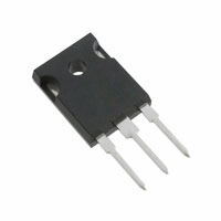
TO-247AC IRG7PH46UPbF
E GC TO-247AD IRG7PH46U-EP
G Gate
C Collector
E Emitter
Absolute Maximum Ratings
Parameter
VCES IC @ TC = 25°C IC @ TC = 100°C INOMINAL ICM ILM VGE PD @ TC = 25°C PD @ TC = 100°C TJ TSTG Collector-to-Emitter Voltage Continuous Collector Current (Silicon Limited) Continuous Collector Current (Silicon Limited) Nominal Current Pulse Collector Current, VGE = 15V Clamped Inductive Load Current, VGE = 20V Continuous Gate-to-Emitter Voltage Maximum Power Dissipation Maximum Power Dissipation Operating Junction and Storage Temperature Range Soldering Temperature, for 10 sec. Mounting Torque, 6-32 or M3 Screw 300 (0.063 in. (1.6mm) from case) 10 lbf·in (1.1 N·m)
Max.
1200 130 75 40
Units
V
g
A
c
120 160 ±30 469 234 -55 to +175 °C V W
Thermal Resistance
Parameter
RθJC (IGBT) RθCS RθJA Thermal Resistance Junction-to-Case-(each IGBT) TO-247AC Thermal Resistance, Case-to-Sink (flat, greased surface)
f
f
Min.
––– ––– –––
Typ.
––– 0.24 40
Max.
0.32 ––– –––
Units
°C/W
Thermal Resistance, Junction-to-Ambient (typical socket mount)
1
www.irf.com
04/20/10
�IRG7PH46UPbF/IRG7PH46U-EP
Electrical Characteristics @ TJ = 25°C (unless otherwise specified)
Parameter
V(BR)CES
∆V(BR)CES/∆TJ
Min.
1200 — — — — 3.0 — — — — —
Typ.
— 1.2 1.7 2.0 2.1 — -15 60 1 1170 —
Max. Units
— — 2.0 — — 6.0 — — 100 — ±200 V V
Conditions
VGE = 0V, IC = 100µA
Collector-to-Emitter Breakdown Voltage
Temperature Coeff. of Breakdown Voltage
e
V/°C VGE = 0V, IC = 1mA (25°C-150°C) IC = 40A, VGE = 15V, TJ = 25°C V IC = 40A, VGE = 15V, TJ IC = 40A, VGE = 15V, TJ VCE = VGE, IC = 1.6mA
VCE(on) VGE(th)
∆VGE(th)/∆TJ
Collector-to-Emitter Saturation Voltage Gate Threshold Voltage Threshold Voltage temp. coefficient Forward Transconductance Collector-to-Emitter Leakage Current Gate-to-Emitter Leakage Current
e d = 150°C d = 175°C d
gfe ICES IGES
mV/°C VCE = VGE, IC = 1.6mA (25°C - 175°C) S VCE = 50V, IC = 40A, PW = 20µs µA nA VGE = 0V, VCE = 1200V VGE = 0V, VCE = 1200V, TJ = 175°C VGE = ±30V
Switching Characteristics @ TJ = 25°C (unless otherwise specified)
Parameter
Qg Qge Qgc Eon Eoff Etotal td(on) tr td(off) tf Eon Eoff Etotal td(on) tr td(off) tf Cies Coes Cres RBSOA Total Gate Charge (turn-on) Gate-to-Emitter Charge (turn-on) Gate-to-Collector Charge (turn-on) Turn-On Switching Loss Turn-Off Switching Loss Total Switching Loss Turn-On delay time Rise time Turn-Off delay time Fall time Turn-On Switching Loss Turn-Off Switching Loss Total Switching Loss Turn-On delay time Rise time Turn-Off delay time Fall time Input Capacitance Output Capacitance Reverse Transfer Capacitance Reverse Bias Safe Operating Area
Min.
— — — — — — — — — — — — — — — — — — — —
Typ.
220 30 85 2560 1780 4340 45 40 410 45 3950 3020 6970 40 40 480 220 4820 150 110
Max. Units
320 50 130 3460 2660 6120 65 55 445 65 — — — — — — — — — — pF ns µJ ns µJ nC IC = 40A
d
Conditions
VGE = 15V VCC = 600V IC = 40A, VCC = 600V, VGE = 15V RG = 10Ω , L = 200µH,TJ = 25°C
d
Energy losses include tail & diode reverse recovery Diode clamp the same as IRG7PH46UDPbF
IC = 40A, VCC = 600V, VGE=15V RG=10Ω , L=200µH, TJ = 175°C
Ãd
Energy losses include tail & diode reverse recovery Diode clamp the same as IRG7PH46UDPbF
VGE = 0V VCC = 30V f = 1.0Mhz IC = 160A VCC = 960V, Vp =1200V Rg = 10Ω , VGE = +20V to 0V, TJ =175°C
FULL SQUARE
Notes:
VCC = 80% (VCES ), VGE = 20V, L = 25µH, RG = 50Ω Pulse width ≤ 400µs; duty cycle ≤ 2%. Refer to AN-1086 for guidelines for measuring V(BR)CES safely. Rθ is measured at TJ of approximately 90°C.
Calculated continuous current based on maximum allowable junction temperature. Bond wire current limit is 117A. Note that current limitations arising from heating of the device leads may occur with some lead mounting arrangements.
2
www.irf.com
�IRG7PH46UPbF/IRG7PH46U-EP
100 For both: Duty cycle : 50% Tj = 150°C Tc = 100°C Vcc = 600V Gate drive as specified Power Dissipation = 154W
Square Wave: VCC
80
Load Current ( A )
60
40
I
20
Diode as specified
0 0.1 1 f , Frequency ( kHz ) 10 100
Fig. 1 - Typical Load Current vs. Frequency
(Load Current = IRMS of fundamental)
140 120 100 80 60 40 20 0 25 50 75 100 T C (°C) 125 150 175
Ptot (W)
500 450 400 350 300 250 200 150 100 50 0 0 20 40 60 80 100 120 140 160 180 T C (°C)
IC (A)
Fig. 2 - Maximum DC Collector Current vs. Case Temperature
1000
Fig. 3 - Power Dissipation vs. Case Temperature
1000
100
10µsec 100µsec
100
IC (A)
IC (A)
10
1msec DC
10
1 Tc = 25°C Tj = 175°C Single Pulse 0.1 1 10 100 VCE (V) 1000 10000
1 10 100 VCE (V) 1000 10000
Fig. 4 - Forward SOA TC = 25°C, TJ ≤ 175°C; VGE =15V
Fig. 5 - Reverse Bias SOA TJ = 175°C; VGE =20V
www.irf.com
3
�IRG7PH46UPbF/IRG7PH46U-EP
160 140 120 100
ICE (A)
160 VGE = 18V VGE = 15V VGE = 12V VGE = 10V VGE = 8.0V 140 120 100
ICE (A)
VGE = 18V VGE = 15V VGE = 12V VGE = 10V VGE = 8.0V
80 60 40 20 0 0 2 4 6 8 10 VCE (V)
80 60 40 20 0 0 2 4 6 8 10 VCE (V)
Fig. 6 - Typ. IGBT Output Characteristics TJ = -40°C; tp =20µs
160 140 120 100 VGE = 18V VGE = 15V VGE = 12V VGE = 10V VGE = 8.0V
Fig. 7 - Typ. IGBT Output Characteristics TJ = 25°C; tp = 20µs
12 10 8
VCE (V)
ICE (A)
80 60 40 20 0 0 2 4 6 8 10 VCE (V)
6 4 2 0 4 8 12
ICE = 20A ICE = 40A ICE = 80A
16
20
VGE (V)
Fig. 8 - Typ. IGBT Output Characteristics TJ = 175°C; tp = 20µs
12 10 8
VCE (V) VCE (V)
Fig. 9 - Typical VCE vs. VGE TJ = -40°C
12 10 8
6 4 2 0 4 8 12
ICE = 20A ICE = 40A ICE = 80A
6 4 2 0
ICE = 20A
ICE = 40A ICE = 80A
16
20
4
8
12 VGE (V)
16
20
VGE (V)
Fig. 10 - Typical VCE vs. VGE TJ = 25°C
Fig. 11 - Typical VCE vs. VGE TJ = 175°C
4
www.irf.com
�IRG7PH46UPbF/IRG7PH46U-EP
160
9200 8200
T J = 25°C
ICE, Collector-to-Emitter Current (A)
140 120 100 80 60 40 20 0 3 4 5 6 7 8 9 VGE, Gate-to-Emitter Voltage (V) T J = 175°C
7200 6200
Energy (µJ)
5200 4200 3200 2200 1200 200 0 10 20 30
EON
EOFF
40 IC (A)
50
60
70
80
Fig. 12- Typ. Transfer Characteristics VCE = 50V; tp = 20µs
1000 tdOFF
Fig. 13 - Typ. Energy Loss vs. IC TJ = 175°C; L = 200µH; VCE = 600V, RG = 10Ω; VGE = 15V
10000
8000
Swiching Time (ns)
Energy (µJ)
tF 100 td ON
EOFF 6000 EON 4000
tR 10 0 10 20 30 40 IC (A) 50 60 70 80
2000 0 25 50 Rg ( Ω) 75 100
Fig. 14 - Typ. Switching Time vs. IC TJ = 175°C; L = 200µH; VCE = 600V, RG = 10Ω; VGE = 15V
10000
Fig. 15 - Typ. Energy Loss vs. RG TJ = 175°C; L = 200µH; VCE = 600V, ICE = 40A; VGE = 15V
Swiching Time (ns)
1000
tdOFF tF
100
tR tdON
10 0 20 40 60 80 100 RG ( Ω)
Fig. 16 - Typ. Switching Time vs. RG TJ = 175°C; L = 200µH; VCE = 600V, ICE = 40A; VGE = 15V
www.irf.com
5
�IRG7PH46UPbF/IRG7PH46U-EP
10000
16
VGE, Gate-to-Emitter Voltage (V)
Cies
14 12 10 8 6 4 2 0
VCES = 600V VCES = 400V
Capacitance (pF)
1000
100
Coes Cres
10 0 100 200 300 VCE (V) 400 500 600
0
50
100
150
200
250
Q G, Total Gate Charge (nC)
Fig. 17 - Typ. Capacitance vs. VCE VGE= 0V; f = 1MHz
Fig. 18- Typical Gate Charge vs. VGE ICE = 40A; L = 2.4mH
1
Thermal Response ( Z thJC )
0.1
D = 0.50 0.20 0.10 0.05
0.01
0.02 0.01
τJ
R1 R1 τJ τ1 τ2
R2 R2
R3 R3 τ3
R4 R4 τC τ τ4
Ri (°C/W)
0.006 0.090 0.142 0.085
τi (sec)
0.000011 0.000177 0.002958
0.001
SINGLE PULSE ( THERMAL RESPONSE )
τ1
τ2
τ3
τ4
Ci= τi/Ri Ci i/Ri
0.015029 Notes: 1. Duty Factor D = t1/t2 2. Peak Tj = P dm x Zthjc + Tc
0.0001 1E-006
1E-005
0.0001
0.001
0.01
0.1
t1 , Rectangular Pulse Duration (sec)
Fig 19. Maximum Transient Thermal Impedance, Junction-to-Case (IGBT) TO-247AC
6
www.irf.com
�IRG7PH46UPbF/IRG7PH46U-EP
L
L
0
DUT 1K
VCC
80 V +
-
DUT Rg
Vclamped
Fig.C.T.1 - Gate Charge Circuit (turn-off)
Fig.C.T.2 - RBSOA Circuit
R = VCC
ICM
DIODE CLAMP
L
DUT / DRIVER
Rg
DUT
VCC
VCC
Rg
Fig.C.T.3 - Switching Loss Circuit
Fig.C.T.4 - Resistive Load Circuit
C f rce o
100K D1 22K
C sense 0.0075µ
Gf orce DUT
E sense
E f rce o
Fig.C.T.5 - BVCES Filter Circuit
www.irf.com
7
�IRG7PH46UPbF/IRG7PH46U-EP
900 800 700 600 500 VCE (V) 400 300 200 100 0 -100 -0.5
Eoff Loss 5% ICE 5% V CE 90% ICE
90 tf 80 70 60 50 VCE (V) I CE (A) 40 30 20 10 0 -10 1.5 2 0 0.5 1
900 800 700 600 500 400 300 200 100 0 -100 -0.3 -0.1
10% test current
tr
TEST CURRENT
90 80 70 60 50 40
90% test current 5% V CE
30 20 10 0 -10
Eon 0.1 0.3 0.5
time(µs)
time (µs)
Fig. WF1 - Typ. Turn-off Loss Waveform @ TJ = 175°C using Fig. CT.4
Fig. WF2 - Typ. Turn-on Loss Waveform @ TJ = 175°C using Fig. CT.4
8
www.irf.com
I CE (A)
�IRG7PH46UPbF/IRG7PH46U-EP
TO-247AC Package Outline
Dimensions are shown in millimeters (inches)
TO-247AC Part Marking Information
@Y6HQG@) UCDTÃDTÃ6IÃDSAQ@"�à XDUCÃ6TT@H7G`à GPUÃ8P9@Ã$%$& 6TT@H7G@9ÃPIÃXXÃ"$�Ã!�� DIÃUC@Ã6TT@H7G`ÃGDI@ÃÅCÅ Ir)ÃÅQÅÃvÃhriyÃyvrÃvv vqvphrÃÅGrhq�A
rrÅ Q6SUÃIVH7@S
,5)3(��
DIU@SI6UDPI6G S@8UDAD@S GPBP 6TT@H7G` GPUÃ8P9@
à "$C $%ÃÃÃÃÃÃÃÃÃÃÃ$&
96U@Ã8P9@ `@6Sà Ã2Ã!�� X@@FÃ"$ GDI@ÃC
TO-247AC package is not recommended for Surface Mount Application. Note: For the most current drawing please refer to IR website at http://www.irf.com/package/
www.irf.com
9
�IRG7PH46UPbF/IRG7PH46U-EP
Dimensions are shown in millimeters (inches)
TO-247AD Package Outline
TO-247AD Part Marking Information
@Y6HQG@) UCDTÃDTÃ6IÃDSBQ"�7 !�F9�@ XDUCÃ6TT@H7G`à GPUÃ8P9@Ã$%$& 6TT@H7G@9ÃPIÃXXÃ"$�Ã!��� DIÃUC@Ã6TT@H7G`ÃGDI@ÃÅCÅ Ir)ÃÅQÅÃvÃhriyÃyvrÃvv vqvphrÃÅGrhq�A
rrÅ DIU@SI6UDPI6G S@8UDAD@S GPBP 6TT@H7G` GPUÃ8P9@ Q6SUÃIVH7@S
Ã�"$C $%ÃÃÃÃÃÃÃÃÃÃÃ$&
96U@Ã8P9@ `@6SÃ�Ã2Ã!��� X@@FÃ"$ GDI@ÃC
TO-247AD package is not recommended for Surface Mount Application. Note: For the most current drawing please refer to IR website at http://www.irf.com/package/ Data and specifications subject to change without notice. This product has been designed and qualified for Industrial market. Qualification Standards can be found on IR’s Web site.
IR WORLD HEADQUARTERS: 233 Kansas St., El Segundo, California 90245, USA Tel: (310) 252-7105 TAC Fax: (310) 252-7903 Visit us at www.irf.com for sales contact information. 04/2010
10
www.irf.com
�